News Posts matching #Lovelace

Return to Keyword Browsing

NVIDIA Allegedly Testing a 900 Watt TGP Ada Lovelace AD102 GPU

With the release of Hopper, NVIDIA's cycle of new architecture releases is not yet over. Later this year, we expect to see next-generation gaming architecture codenamed Ada Lovelace. According to a well-known hardware leaker for NVIDIA products, @kopite7kimi, on Twitter, the green team is reportedly testing a potent variant of the upcoming AD102 SKU. As the leak indicates, we could see an Ada Lovelace AD102 SKU with a Total Graphics Power (TGP) of 900 Watts. While we don't know where this SKU is supposed to sit in the Ada Lovelace family, it could be the most powerful, Titan-like design making a comeback. Alternatively, this could be a GeForce RTX 4090 Ti SKU. It carries 48 GB of GDDR6X memory running at 24 Gbps speeds alongside monstrous TGP. Feeding the card are two 16-pin connectors.

Another confirmation from the leaker is that the upcoming RTX 4080 GPU uses the AD103 SKU variant, while the RTX 4090 uses AD102. For further information, we have to wait a few more months and see what NVIDIA decides to launch in the upcoming generation of gaming-oriented graphics cards.

NVIDIA GeForce RTX 4090/4080 to Feature up to 24 GB of GDDR6X Memory and 600 Watt Board Power

After the data center-oriented Hopper architecture launch, NVIDIA is slowly preparing to transition the consumer section to new, gaming-focused designs codenamed Ada Lovelace. For starters, the source claims that NVIDIA is using the upcoming GeForce RTX 3090 Ti GPU as a test run for the next-generation Ada Lovelace AD102 GPU. Thanks to the authorities over at Igor's Lab, we have some additional information about the upcoming lineup. We have a sneak peek of a few features regarding the top-end GeForce RTX 4080 and RTX 4090 GPU SKUs. According to Igor's claims, NVIDIA is testing the PCIe Gen5 power connector and wants to see how it fares with the biggest GA102 SKU - GeForce RTX 3090 Ti.

Additionally, we find that the AD102 GPU is supposed to be pin-compatible with GA102. This means that the number of pins located on GA102 is the same as what we are going to see on AD102. There are 12 places for memory modules on the AD102 reference design board, resulting in up to 24 GB of GDDR6X memory. As much as 24 voltage converters surround the GPU, NVIDIA will likely implement uP9512 SKU. It can drive eight phases, resulting in three voltage converters per phase, ensuring proper power delivery. The total board power (TBP) is likely rated at up to 600 Watts, meaning that the GPU, memory, and power delivery combined output 600 Watts of heat. Igor notes that board partners will bundle 12+4 (12VHPWR) to four 8-pin (PCIe old) converters to enable PSU compatibility.

NVIDIA GeForce RTX 3090 Ti Coming Out by March-End, 16GB RTX 3070 Ti Canned?

NVIDIA is finally coming around to launching its top-of-the-line GeForce RTX 3090 Ti "Ampere" graphics card on March 29, 2022, according to a source on the ChipHell community, cited by Wccftech. The same source also mentions that NVIDIA has dropped the idea of releasing a 16 GB variant of the performance-segment GeForce RTX 3070 Ti, which means the company is possibly wrapping up the its RTX 30-series "Ampere" product-stack updates going into Spring-Summer, so it could prepare for its next-generation RTX 40-series based on the "Ada Lovelace" graphics architecture, with mid-year announcements followed by product launches in the second half of 2022.

NVIDIA Increases Caches for Ada Lovelace, to Catch Up with AMD

The next-generation "Ada Lovelace" graphics architecture powering NVIDIA's GeForce RTX 40-series graphics cards, could see a significant increase in on-die cache memory, according to leaked source-code related to drivers or firmware, seen by XinoAssassin on Twitter. The source-code leak emanates from the recent large-scale cyber-attack on NVIDIA. When comparing source files related to Ampere and Ada architectures, XinoAssassin noticed lines that reference large cache slices.

From this, it was analyzed that the top-of-the-line AD102 silicon will have 96 MB of last-level cache on the silicon; the AD103 and AD104 chips have 64 MB; the AD106 has 48 MB, and the smallest AD107 has 32 MB. Compare this to the 6 MB on the GA102, puny 4 MB on the GA103 and GA104; 3 MB on the GA106, and 2 MB on the GA107. NVIDIA is known to make innovations in generational memory bandwidth increase and memory management, with each new architecture. The company could tap into even faster versions of GDDR6X memory it co-developed with Micron (GDDR6 with PAM4 signaling).

NVIDIA "Ada Lovelace" Streaming Multiprocessor Counts Surface

Possible streaming multiprocessor (SM) counts of the various NVIDIA "Ada Lovelace" client-graphics GPUs surfaced, allegedly pieced together from code seen in the recent NVIDIA cyberattack data-leak. According to this, the top-dog "AD102" silicon has 144 SM, the next-best "AD103" has 84. The third-largest "AD104" silicon has 60. The performance-segment "AD106" has 36, and the mainstream "AD107" has 24. Assuming the number of CUDA cores per SM in the "Ada Lovelace" graphics architecture is unchanged from that of "Ampere," we're looking at 18,432 CUDA cores for the "AD102," an impressive 10,752 for the "AD103," 7,680 cores for the "AD104," 4,608 for the "AD106," and 3,072 for the "AD107."

NVIDIA to Split Graphics and Compute Architecture Naming, "Blackwell" Architecture Spotted

The recent NVIDIA data-leak springs up information on various upcoming graphics parts. Besides "Ada Lovelace," "Hopper," we come across a new codename, "Blackwell." It turns out that NVIDIA is splitting the the graphics and compute architecture naming with the next generation, not unlike what AMD did, with its RDNA and CDNA series. The current "Ampere" architecture is being used both for compute and graphics, with the streaming multiprocessor for the two being slightly different—the compute "Ampere" has more FP64 and Tensor components, while the graphics "Ampere" does away with these in favor of RT cores and graphics-relevant components.

The graphics architecture to succeed GeForce "Ampere" will be GeForce "Ada Lovelace." GPUs in this series are identified in the leaked code as "AD102," "AD103," "AD104," "AD106," "AD107," and "AD10B," succeeding a similar numbering for parts with the "A" (GeForce Ampere) series. The compute architecture succeeding "Ampere" will be codenamed "Hopper." with parts in the series being codenamed "GH100" and "GH202." Another compute or datacenter architecture is "Blackwell," with parts being codenamed "GB100" and "GB102." From all accounts, NVIDIA is planning to launch the GeForce 40-series "Ada" graphics card lineup in the second half of 2022. The company is in need of a similar refresh for its compute product lineup, and could debut "Hopper" either toward the end of 2022 or next year. "Blackwell" could follow "Hopper."

NVIDIA Rumored to Refresh RTX 30-series with SUPER SKUs in January, RTX 40-series in Q4-2022

NVIDIA is rumored to be giving its GeForce RTX 30-series "Ampere" graphics card family a mid-term refresh by the 2022 International CES, in January; the company is also targeting Q4-2022, specifically October, to debut its next-generation RTX 40-series. The Q1 refresh will include "SUPER" branded SKUs taking over key price-points for NVIDIA, as it lands up with enough silicon that can be fully unlocked. This leak comes from Greymon55, a reliable source on NVIDIA leaks. It also aligns with the most recent pattern followed by NVIDIA to keep its GeForce product-stack updated. The company had recently released "Ti" updates to certain higher-end price-points, in response to competition from the Radeon RX 6000 "RDNA2" series.

NVIDIA's next-generation will be powered by the "Lovelace" graphics architecture that sees even more hardware acceleration for the RTX feature-set, more raytraced effects, and preparation for future APIs. It also marks NVIDIA's return to TSMC, with the architecture reportedly being designed for the 5 nm (N5) silicon fabrication node. The current-gen GeForce "Ampere" chips are being products on an 8 nm foundry node by Samsung.

Intel's "Alder Lake" Desktop Processor supports DDR4+DDR5, (only few) PCIe Gen 5 and Dynamic Memory Clock

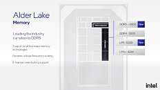
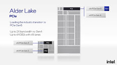
Intel will beat AMD to next-generation I/O, with its 12th Generation Core "Alder Lake-S" desktop processors. The company confirmed that the processor will debut both DDR5 memory and PCI-Express Gen 5.0, which double data-rates over current-gen DDR4 and PCI-Express Gen 4, respectively. "Alder Lake-S" features a dual-channel DDR5 memory interface, with data-rates specced to DDR5-4800 MHz, more with overclocking, reaching enthusiast-grade memory attaining speeds in excess of DDR5-7200. Besides speed, DDR5 is expected to herald a doubling in density, with 16 GB single-rank modules becoming a common density-class, 32 GB single-rank being possible in premium modules; and 64 GB dual-rank modules being possible soon. Leading memory manufacturers have started announcing their first DDR5 products in preparation of "Alder Lake-S" launch in Q4-2021.

The memory controller is now able to dynamically adjust memory frequency and voltage, depending on current workload, power budget and other inputs—a first for the PC! This could even mean automatic "Turbo" overclocking for memory. Intel also mentioned "Enhanced Overclocking Support" but didn't go into further detail what that entails. While DDR5 is definitely the cool new kid on the block, Intel's Alder Lake memory controller keeps support for DDR4, and LPDDR4, while adding LPDDR5-5200 support (important for mobile devices). Just to clarify, there won't be one die support DDR5, and another for DDR4, no, all dies will have support for all four of these memory standards. How that will work out for motherboard designs is unknown at this point.

Chip Shortages Could Continue Well into 2022, Predicts NVIDIA CEO Jensen Huang

In his Q2-FY2022 Results call, NVIDIA CEO Jensen Huang commented that he expects the ongoing chip supply situation to remain bad for the most part of 2022. "Meanwhile, we have and are securing pretty significant long-term supply commitments as we expand into all these different markets initiatives that we've set ourselves up for. And I so I think—I would expect that we will see a supply contained environment for the vast majority of next year is my guess at the moment," he said.

His comments are telling, as NVIDIA relies heavily on cutting edge silicon fabrication nodes for its logic products, such as GPUs, HPC processors, and vehicle SoCs. 2022 will see NVIDIA introduce its "Lovelace" graphics architecture, powering the GeForce RTX 40-series GPUs; as well as a variant powering next-generation HPC processors. The company is looking to design its chips for TSMC's 5 nm silicon fabrication process, unless Samsung can fix its 5 nm-class foundry woes in time, and win back the company.

NVIDIA "Ada Lovelace" Architecture Designed for N5, GeForce Returns to TSMC

NVIDIA's upcoming "Ada Lovelace" architecture, both for compute and graphics, is reportedly being designed for the 5 nanometer silicon fabrication node by TSMC. This marks NVIDIA's return to the Taiwanese foundry after its brief excursion to Samsung, with the 8 nm "Ampere" graphics architecture. "Ampere" compute dies continue to be built on TSMC 7 nm nodes. NVIDIA is looking to double the compute performance on its next-generation GPUs, with throughput approaching 70 TFLOP/s, from a numeric near-doubling in CUDA cores, generation-over-generation. These will also be run at clock speeds above 2 GHz. One can expect "Ada Lovelace" only by 2022, as TSMC N5 matures.

Next-Generation Nintendo Switch SoC to be Powered by NVIDIA's Ada Lovelace GPU Architecture

Nintendo's Switch console is one of the most successful consoles ever made by the Japanese company. It has sold in millions of units and has received great feedback from the gaming community. However, as the hardware inside the console becomes outdated, the company is thinking about launching a new revision of the console, with the latest hardware and technologies. Today, we got ahold of information about the graphics side of things in Nintendo's upcoming console. Powered by NVIDIA Tegra SoC, it will incorporate unknown Arm-based CPU cores. The latest rumors suggest that the CPU will be accommodated with NVIDIA's Ada Lovelace GPU architecture. According to @kopite7kimi, a known hardware leaker, who simply replied to VideoCardz's tweet with "Ada", we are going to see the appearance of Ada Lovelace GPU architecture in the new SoC. Additionally, the new Switch SoC will have hardware accelerated NVIDIA Deep Learning Super Sampling (DLSS) and 4K output.

NVIDIA's Next-Gen Big GPU AD102 Features 18,432 Shaders

The rumor mill has begun grinding with details about NVIDIA's next-gen graphics processors based on the "Lovelace" architecture, with Kopite7kimi (a reliable source with NVIDIA leaks) predicting a 71% increase in shader units for the "AD102" GPU that succeeds the "GA102," with 12 GPCs holding 6 TPCs (12 SMs), each. 3DCenter.org extrapolates on this to predict a CUDA core count of 18.432 spread across 144 streaming multiprocessors, which at a theoretical 1.80 GHz core clock could put out an FP32 compute throughput of around 66 TFLOP/s.

The timing of this leak is interesting, as it's only 3 months into the market cycle of "Ampere." NVIDIA appears unsettled with AMD RDNA2 being competitive with "Ampere" at the enthusiast segment, and is probably bringing in its successor, "Lovelace" (after Ada Lovelace), out sooner than expected. Its previous generation "Turing" architecture saw market presence for close to two years. "Lovelace" could leverage the 5 nm silicon fabrication process and its significantly higher transistor density, to step up performance.

NVIDIA to Introduce an Architecture Named After Ada Lovelace, Hopper Delayed?

NVIDIA has launched its GeForce RTX 3000 series of graphics cards based on the Ampere architecture three months ago. However, we are already getting information about the next-generation that the company plans to introduce. In the past, the rumors made us believe that the architecture coming after Ampere is allegedly being called Hopper. Hopper architecture is supposed to bring multi-chip packaging technology and be introduced after Ampere. However, thanks to @kopite7kimi on Twitter, a reliable source of information, we have data that NVIDIA is reportedly working on a monolithic GPU architecture that the company internally refers to as "ADxxx" for its codenames.

The new monolithically-designed Lovelace architecture is going make a debut on the 5 nm semiconductor manufacturing process, a whole year earlier than Hopper. It is unknown which foundry will manufacture the GPUs, however, both of NVIDIA's partners, TSMC and Samsung, are capable of manufacturing it. The Hopper is expected to arrive sometime in 2023-2024 and utilize the MCM technology, while the Lovelace architecture will appear in 2021-2022. We are not sure if the Hopper architecture will be exclusive to data centers or extend to the gaming segment as well. The Ada Lovelace architecture is supposedly going to be a gaming GPU family. Ada Lovelace, a British mathematician, has appeared on NVIDIA's 2018 GTC t-shirt known as "Company of Heroes", so NVIDIA may have already been using the ADxxx codenames internally for a long time now.
Return to Keyword Browsing
Dec 18th, 2024 05:00 EST change timezone

New Forum Posts

Popular Reviews

Controversial News Posts