News Posts matching #Mark Papermaster

Return to Keyword Browsing

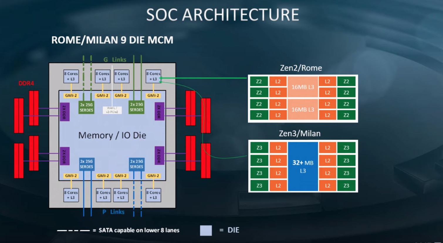
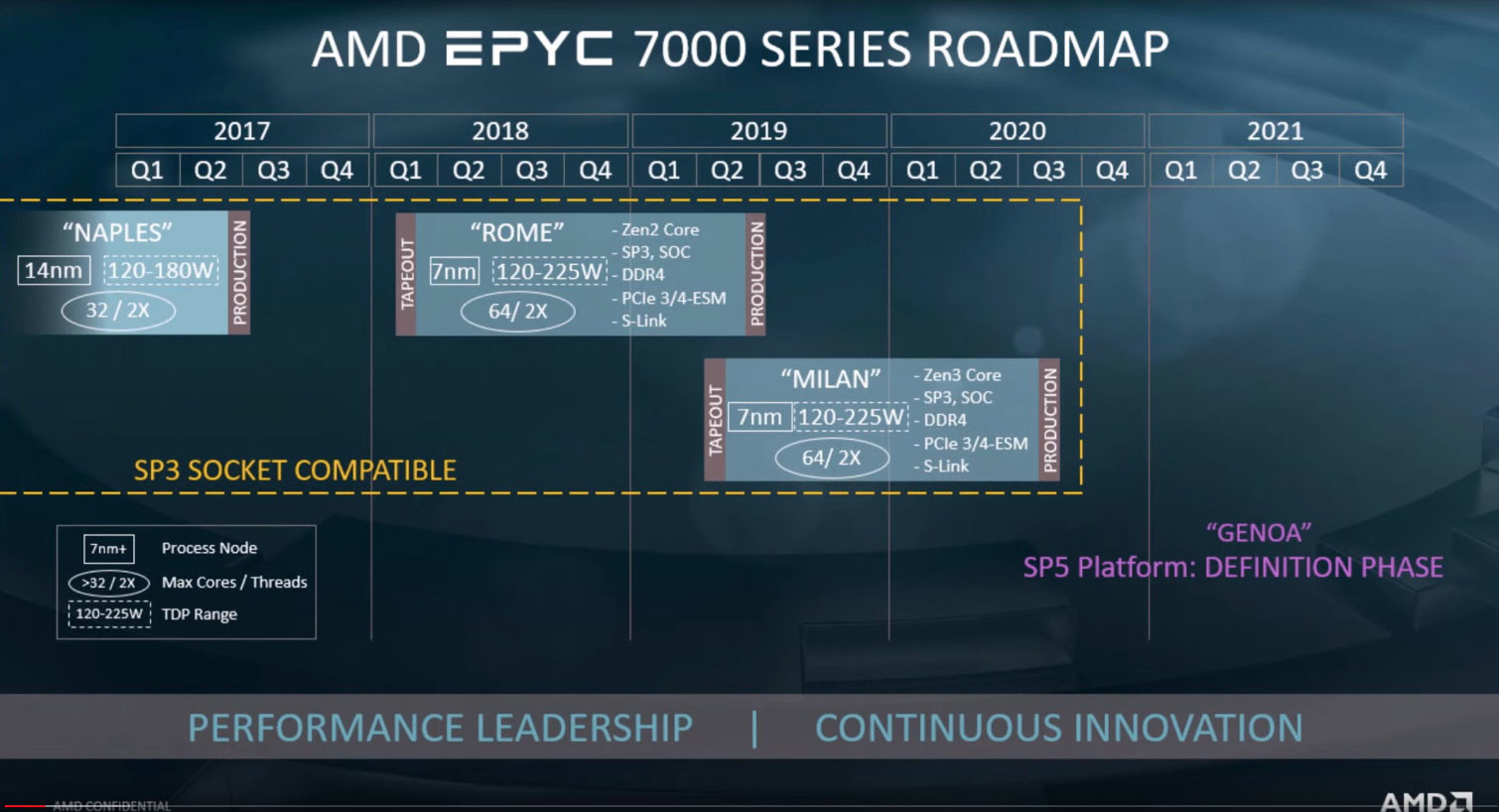
AMD CTO Teases Memory Upgrades for Revised Instinct MI300-series Accelerators

Brett Simpson, Partner and Co-Founder of Arete Research, sat down with AMD CTO Mark Papermaster during the former's "Investor Webinar Conference." A transcript of the Arete + AMD question and answer session appeared online last week—the documented fireside chat concentrated mostly on "AI compute market" topics. Papermaster was asked about his company's competitive approach when taking on NVIDIA's very popular range of A100 and H100 AI GPUs, as well as the recently launched GH200 chip. The CTO did not reveal any specific pricing strategies—a "big picture" was painted instead: "I think what's important when you just step back is to look at total cost of ownership, not just one GPU, one accelerator, but total cost of ownership. But now when you also look at the macro, if there's not competition in the market, you're going to see not only a growth of the price of these devices due to the added content that they have, but you're -- without a check and balance, you're going to see very, very high margins, more than that could be sustained without a competitive environment."

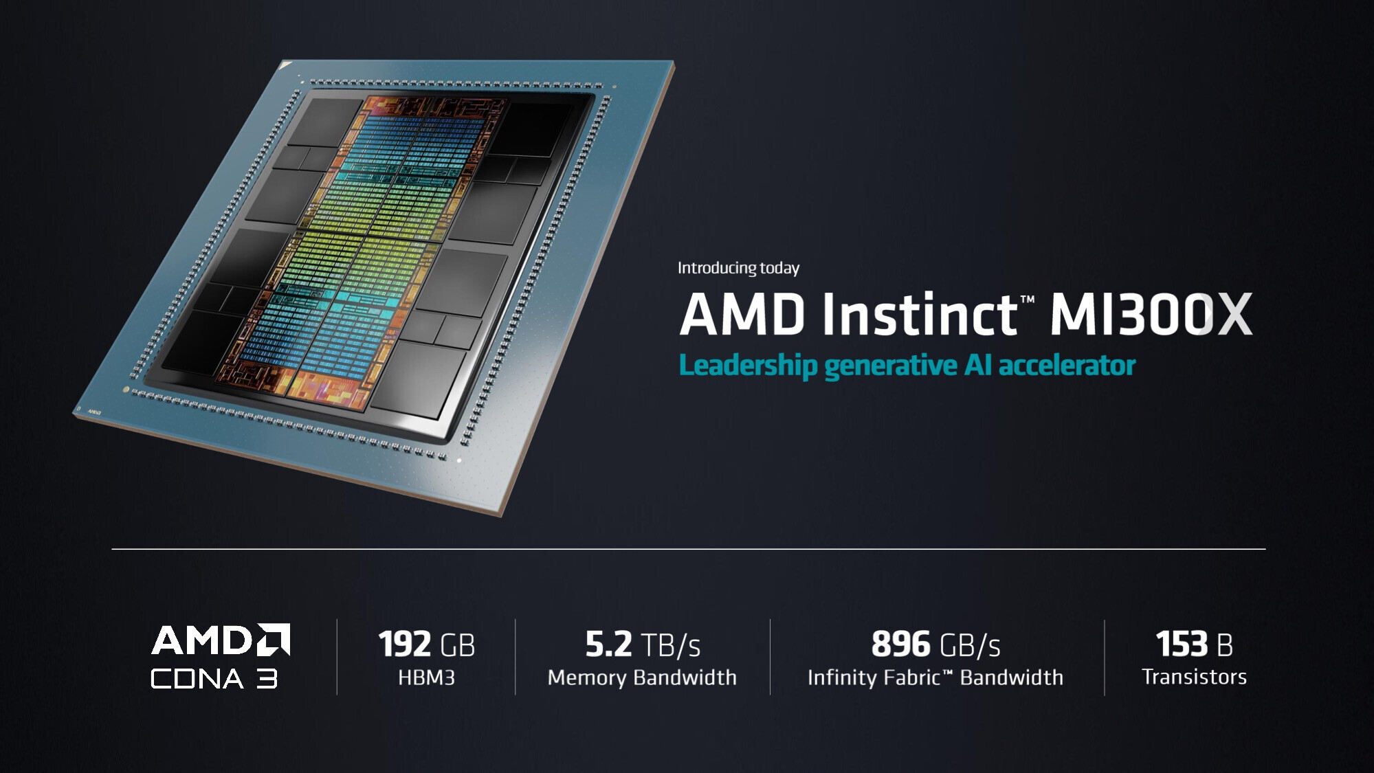
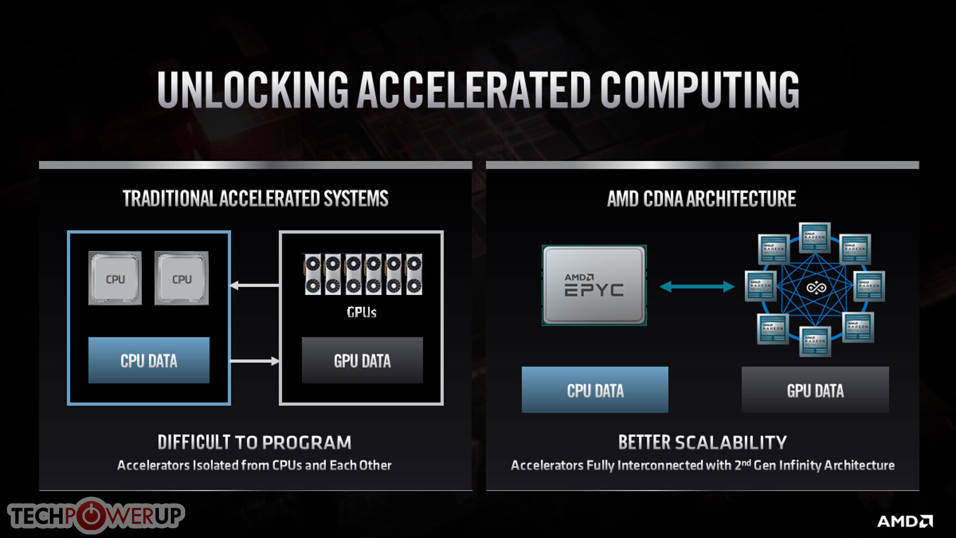
Papermaster continued: "And what I think is very key with -- as AMD has brought competition market for these most powerful AI training and inference devices is you will see that check and balance. And we have a very innovative approach. We've been a leader in chiplet design. And so we have the right technology for the right purpose of the AI build-out that we do. We have, of course, a GPU accelerator. But there's many other circuitry associated with being able to scale and build out these large clusters, and we're very, very efficient in our design." Team Red started to ship its flagship accelerator, Instinct MI300X, to important customers at the start of 2024—Arete Research's Simpson asked about the possibility of follow-up models. In response, AMD's CTO referenced some recent history: "Well, I think the first thing that I'll highlight is what we did to arrive at this point, where we are a competitive force. We've been investing for years in building up our GPU road map to compete in both HPC and AI. We had a very, very strong harbor train that we've been on, but we had to build our muscle in the software enablement."

AMD Announces Plan to Invest Approximately $400 Million Over the Next Five Years in India

AMD today announced plans for continued growth in India through an approximate $400M investment over the next five years. The planned investment includes a new AMD campus in Bangalore, Karnataka that will serve as the company's largest design center, as well as the addition of approximately 3,000 new engineering roles by the end of 2028. The new AMD campus is expected to open before the end of 2023 and will feature extensive lab space, state-of-the-art collaboration tools and seating configurations designed to foster teamwork. The investment is supported by the various policy initiatives of the Government of India focused on the semiconductor industry.

"We welcome the AMD plan to expand its leading-edge R&D engineering operations in India," said Mr. Ashwini Vaishnaw, Union Cabinet Minister for Railways, Telecommunications, Electronics and Information Technology, Government of India. "I welcome AMD's decision to set up its largest R&D design center in India and expansion of the India-AMD partnership. It will certainly play an important role in building a world class semiconductor design and innovation ecosystem. It will also provide tremendous opportunities for our large pool of highly skilled semiconductor engineers and researchers and will catalyse PM Narendra Modi's vision of India becoming a global talent hub," said Mr. Rajeev Chandrasekhar, Minister of State for Electronics and IT, Skill Development and Entrepreneurship.

AMD CEO Lisa Su Notes: AI to Dominate Chip Design

Artificial intelligence (AI) has emerged as a transformative force in chip design, with recent examples from China and the United States showcasing its potential. Jensen Huang, CEO of Nvidia, believes that AI can empower individuals to become programmers, while Lisa Su, CEO of AMD, predicts an era where AI dominates chip design. During the 2023 World Artificial Intelligence Conference (WAIC) in Shanghai, Su emphasized the importance of interdisciplinary collaboration for the next generation of chip designers. To excel in this field, engineers must possess a holistic understanding of hardware, software, and algorithms, enabling them to create superior chip designs that meet system usage, customer deployment, and application requirements.

The integration of AI into chip design processes has gained momentum, fueled by the AI revolution catalyzed by large language models (LLMs). Both Huang and Mark Papermaster, CTO of AMD, acknowledge the benefits of AI in accelerating computation and facilitating chip design. AMD has already started leveraging AI in semiconductor design, testing, and verification, with plans to expand its use of generative AI in chip design applications. Companies are now actively exploring the fusion of AI technology with Electronic Design Automation (EDA) tools to streamline complex tasks and minimize manual intervention in chip design. Despite limited data and accuracy challenges, the "EDA+AI" approach holds great promise. For instance, Synopsys has invested significantly in AI tool research and recently launched Synopsys.ai, the industry's first end-to-end AI-driven EDA solution. This comprehensive solution empowers developers to harness AI at every stage of chip development, from system architecture and design to manufacturing, marking a significant leap forward in AI's integration into chip design workflows.

AMD Still Believes in Moore's Law, Unlike NVIDIA

Back in September, NVIDIA's Jensen Huang said that Moore's Law is dead, but it seems like AMD disagrees with NVIDIA, at least for now. According to an interview with AMD's CTO, Mark Papermaster, AMD still believes that Moore's Law will be alive for another six to eight years. However, AMD no longer believes that transistor density can be doubled every 18 to 24 months, while remaining in the same cost envelope. "I can see exciting new transistor technology for the next - as far as you can really plot these things out - about six to eight years, and it's very, very clear to me the advances that we're going to make to keep improving the transistor technology, but they're more expensive," Papermaster said.

AMD believes we'll see a change in how chips are being designed and put together, with chiplets being the future of semiconductors. Papermaster calls this "a Moore's Law equivalent, meaning that you continue to really double that capability every 18 to 24 months" although it's not exactly Moore's Law in the traditional sense. AMD also appears to be betting heavily on FPGA technology in some of its market segments, for something the company calls adaptive computing. As to how things will play out, time will tell, but with both AMD and Intel going down the chiplet route, albeit in slightly different ways, we should continue to see new innovations from both companies, with or without Moore's Law.

AMD to Host Livestream Event on the 29th of August to Unveil Next Generation Ryzen Processors

Today, AMD (NASDAQ: AMD) announced "together we advance_PCs," a livestream premiere to unveil next generation AMD PC products. Chair and CEO Dr. Lisa Su, CTO and EVP Mark Papermaster, and other AMD executives will present details on the latest "Zen 4" architecture that powers upcoming AMD Ryzen processors and the all new AM5 platform built around the latest technologies including DDR5 and PCIe 5.0, all designed to drive a new era of performance desktop PCs.

The show will premiere at 7 p.m. ET on Monday, August 29, on the AMD YouTube channel. A replay can be accessed a few hours after the conclusion of the event at AMD.com/Ryzen.

AMD Will Give a Glimpse of Zen4 Core at CES 2022 Presentation

As the year ends, one of the biggest consumer trade shows, CES, is on the horizon, and manufacturers are ready to present the work that will become real throughout the year. AMD will offer a keynote at the CES 2022 press conference, and we expect to hear more about the upcoming Zen3 processors with 3D V-cache stacked in them. However, what is interesting is that we may listen to more details about Zen4 core. In an exclusive interview conducted by Antony Leather, Forbes contributor and the person behind CrazyTechLab, AMD CTO Mark Papermaster started the hype machine by sharing that AMD will announce some Zen4 core details at the CES 2022 conference.
AMD CTO Mark PapermasterWith regards to the upcoming generation - I point to CES in January. We're excited to be revealing some additional details on our new product launches that will deliver phenomenal experiences and as we've said, later in the year as it progresses we'll share more detail on Zen 4 with some mentioned at CES and more announcements on it over the course of 2022. It will be a very exciting year for AMD.

AMD Promotes Methodology Architect Alex Starr to Corporate Fellow

AMD today announced the appointment of methodology architect Alex Starr to AMD Corporate Fellow. The appointment recognizes Starr for his outstanding technical leadership and contributions pioneering advanced emulation methodologies that have accelerated product validation processes, reduced time to market and improved the overall quality of AMD products.

"Alex played a significant role placing AMD at the forefront of hardware emulation and virtual platform technology," said Mark Papermaster, chief technology officer and executive vice president of Technology and Engineering at AMD. "The strategies and methodologies developed under his leadership have been adopted across all of AMD and are a defining marker in our company's culture of innovation. As a result of Alex and the team's efforts, we have significantly reduced silicon bring-up time and silicon revisions, enabling AMD to consistently bring our leadership products to market faster."

Starr, an AMD veteran of nearly 15 years, is an esteemed leader in verification methodologies for CPU and GPU processors and complex SoCs. His deep industry experience and innovations have enabled AMD to continue executing on its technology roadmap and enhancing its competitive position within the industry.

AMD Confirms CDNA-Based Radeon Instinct MI100 Coming to HPC Workloads in 2H2020

Mark Papermaster, chief technology officer and executive vice president of Technology and Engineering at AMD, today confirmed that CDNA is on-track for release in 2H2020 for HPC computing. The confirmation was (adequately) given during Dell's EMC High-Performance Computing Online event. This confirms that AMD is looking at a busy 2nd half of the year, with both Zen 3, RDNA 2 and CDNA product lines being pushed to market.

CDNA is AMD's next push into the highly-lucrative HPC market, and will see the company differentiating their GPU architectures through market-based product differentiation. CDNA will see raster graphics hardware, display and multimedia engines, and other associated components being removed from the chip design in a bid to recoup die area for both increased processing units as well as fixed-function tensor compute hardware. CNDA-based Radeon Instinct MI100 will be fabricated under TSMC's 7 nm node, and will be the first AMD architecture featuring shared memory pools between CPUs and GPUs via the 2nd gen Infinity Fabric, which should bring about both throughput and power consumption improvements to the platform.

AMD Financial Analyst Day 2020 Live Blog

AMD Financial Analyst Day presents an opportunity for AMD to talk straight with the finance industry about the company's current financial health, and a taste of what's to come. Guidance and product teasers made during this time are usually very accurate due to the nature of the audience. In this live blog, we will post information from the Financial Analyst Day 2020 as it unfolds.
20:59 UTC: The event has started as of 1 PM PST. CEO Dr Lisa Su takes stage.

AMD Zen 3 Could Bid the CCX Farewell, Feature Updated SMT

With its next-generation "Zen 3" CPU microarchitecture designed for the 7 nm EUV silicon fabrication process, AMD could bid the "Zen" compute complex or CCX farewell, heralding chiplets with monolithic last-level caches (L3 caches) that are shared across all cores on the chiplet. AMD embraced a quad-core compute complex approach to building multi-core processors with "Zen." At the time, the 8-core "Zeppelin" die featured two CCX with four cores, each. With "Zen 2," AMD reduced the CPU chiplet to only containing CPU cores, L3 cache, and an Infinity Fabric interface, talking to an I/O controller die elsewhere on the processor package. This reduces the economic or technical utility in retaining the CCX topology, which limits the amount of L3 cache individual cores can access.

This and more juicy details about "Zen 3" were put out by a leaked (later deleted) technical presentation by company CTO Mark Papermaster. On the EPYC side of things, AMD's design efforts will be spearheaded by the "Milan" multi-chip module, featuring up to 64 cores spread across eight 8-core chiplets. Papermaster talked about how the individual chiplets will feature "unified" 32 MB of last-level cache, which means a deprecation of the CCX topology. He also detailed an updated SMT implementation that doubles the number of logical processors per physical core. The I/O interface of "Milan" will retain PCI-Express gen 4.0 and eight-channel DDR4 memory interface.

AMD Zen 2 EPYC "Rome" Launch Event Live Blog

AMD invited TechPowerUp to their launch event and editor's day coverage of Zen 2 EPYC processors based on the 7 nm process. The event was a day-long affair which included product demos and tours, and capped off with an official launch presentation which we are able to share with you live as the event goes on. Zen 2 with the Ryzen 3000-series processors ushered in a lot of excitement, and for good reason too as our own reviews show, but questions remained on how the platform would scale to the other end of the market. We already knew, for example, that AMD secured many contracts based on their first-generation EPYC processors, and no doubt the IPC increase and expected increased core count would cause similar, if not higher, interest here. We also expect to know shortly about the various SKUs and pricing involved, and also if AMD wants to shed more light on the future of the Threadripper processor family. Read below, and continue past the break, for our live coverage.
21:00 UTC: Lisa Su is on the stage at the Palace of Fine Arts events venue in San Francisco to present AMD's latest developments on EPYC for datacenters, using the Zen 2 microarchitecture.

21:10 UTC: AMD focuses not just on delivering a single chip, but it's goal is to deliver a complete solution for the enterprise.

AMD Zen3 to Leverage 7nm+ EUV For 20% Transistor Density Increase

AMD "Zen 3" microarchitecture could be designed for the enhanced 7 nm+ EUV (extreme ultraviolet) silicon fabrication node at TSMC, which promises a significant 20 percent increase in transistor densities compared to the 7 nm DUV (deep ultraviolet) node on which its "Zen 2" processors are being built. In addition, the node will also reduce power consumption by up to 10 percent at the same operational load. In a late-2018 interview, CTO Mark Papermaster stated AMD's design goal with "Zen 3" would be to prioritize energy-efficiency, and that it would present "modest" performance improvements (read: IPC improvements) over "Zen 2." AMD made it clear that it won't drag 7 nm DUV over more than one microarchitecture (Zen 2), and that "Zen 3" will debut in 2020 on 7 nm+ EUV.

AMD Re-structures Leadership Team; James Prior Leaves AMD

Let me be the first to say that the two may not be directly related, but it is an awfully strong coincidence that both pieces of news come out on the same day. Indeed, earlier in the day AMD put out a press release (full release past the break) announcing "multiple organizational changes focused on strengthening the company's senior leadership team and accelerating growth." Several familiar names have been promoted within the company to be in charge of more products and visions across their CPU and GPU business units. Mark Papermaster, for example, is now an executive VP as well as CTO of AMD, and the company has also hired in new talent, including industry veteran Sandeep Chennakeshu, as executive VP of "Computing and Graphics responsible for the company's high-performance PC, gaming and semi-custom businesses".

Perhaps all this re-structuring and new hiring comes in handy, at a time when we have seen several people leave AMD for Intel or otherwise. Indeed, shortly after that press release went out, word got to us that James Prior, Senior Product Manager for AMD, and an ardent employee for nearly 6 years, is no longer working for the company. We have no word yet on what is next for James, but it was more than a small surprise to know that the person you just spoke with at CES, and had a long conversation of AMD's desktop processors, is gone just like that. We have known James for many years now, and can attest to his work ethics as well as being a great guy all-round. We wish him the best in his future ventures, and look forward to also seeing how AMD's re-structuring turns out.

AMD CTO Mark Papermaster Confirms 7 nm Lineup Refresh for 2019

AMD's CTO Mark Papermaster, in an interview with TheStreet, confirmed AMD's plans with 7 nm for their graphics offerings are just beginning with Radeon VII. When inquired on AMD's plans for their graphics division, Papermaster said that "What we do over the course of the year is what we do every year. We'll round out the whole roadmap." he then added that "We're really excited to start on the high-end... you'll see the announcements over the course of the year as we round out our Radeon roadmap."

So these comments form papermaster seemingly confirm two things: first, that AMD plans to "round out" its lineup using the 7 nm process technology, which means increasing offerings at different price points. The use of the word "refresh" almost takes the breath away, since refreshes are usually based on the same previous architectures. However, AMD does have plans for a new mid-range chip to finally succeed Polaris in Navi, which should become the next AMD launch in the 7 nm process for graphics technologies.

AMD and Xilinx Announce a New World Record for AI Inference

At today's Xilinx Developer Forum in San Jose, Calif., our CEO, Victor Peng was joined by the AMD CTO Mark Papermaster for a Guinness. But not the kind that comes in a pint - the kind that comes in a record book. The companies revealed the AMD and Xilinx have been jointly working to connect AMD EPYC CPUs and the new Xilinx Alveo line of acceleration cards for high-performance, real-time AI inference processing. To back it up, they revealed a world-record 30,000 images per-second inference throughput!

The impressive system, which will be featured in the Alveo ecosystem zone at XDF today, leverages two AMD EPYC 7551 server CPUs with its industry-leading PCIe connectivity, along with eight of the freshly-announced Xilinx Alveo U250 acceleration cards. The inference performance is powered by Xilinx ML Suite, which allows developers to optimize and deploy accelerated inference and supports numerous machine learning frameworks such as TensorFlow. The benchmark was performed on GoogLeNet, a widely used convolutional neural network.

AMD "Navi" GPU Architecture Successor Codenamed "Arcturus"?

Arcturus is the fourth brightest star in the night sky, and could be the a new GPU architecture by AMD succeeding "Navi," according to a Phoronix report. The codename of Navi-successor has long eluded AMD's roadmap slides. The name "Arcturis" surfaced on Phoronix community forums, from a post by an AMD Linux liaison who is a member there. The codename is also supported by the fact that AMD is naming its GPU architectures after the brightest stars in the sky (albeit in a descending order of their brightness). Polaris is the brightest, followed by Vega, Navi, and Arcturus.

AMD last referenced the Navi-successor on a roadmap slide during its 2017 Financial Analyst Day presentation by Mark Papermaster. That slide mentioned "Vega" to be built on two silicon fabrication processes, 14 nm and "14 nm+." We know now that AMD intends to build a better-endowed "Vega" chip on 7 nm, which could be the world's first 7 nm GPU. "Navi" is slated to be built on 7 nm as the process becomes more prevalent in the industry. The same slide mentions Navi-successor as being built on "7 nm+," which going by convention, could refer to an even more advanced process than 7 nm. Unfortunately, even in 2017, when the industry was a touch more optimistic about 7 nm, AMD expected the Navi-successor to only come out by 2020. We're not holding our breath.

AMD Chip Manufacturing to Lay Solely With TSMC On, After 7 nm - And Why It's not a Decision, but a Necessity

It's been a tumultuous few days for AMD, as the company has seen Jim Anderson, Computing and Graphics Group leader after the departure of Raja Koduri, leave the company, at a time of soaring share value for the company (hitting $25.26 and leaving short positions well, short, by $2.67 billion.) However, there's one particular piece of news that is most relevant for the company: Globalfoundries' announcement to stop all ongoing development on the 7 nm node.

This is particularly important for a variety of reasons. The most important one is this: Globalfoundries' inability to execute on the 7 nm node leaves AMD fully free to procure chips and technology from competing foundries. If you remember, AMD's spin-off of GlobalFoundries left the former with the short end of the stick, having to cater to GlobalFoundries' special pricing, and paying for the privilege of accessing other foundries' inventories. Of course, the Wafer Supply Agreement (WSA) that is in place will have to be amended - again - but the fact is this: AMD wants 7 nm products, and GlobalFoundries can't provide.
To the forumites: this piece is marked as an editorial

Rollercoaster Monday for AMD as it Loses Jim Anderson, Closes Above $25 in Stock Price

It has been a rollercoaster Monday for AMD as it bled yet another bright executive. Jim Anderson, who led Computing and Graphics Group after the departure of Raja Koduri, and who is rumored to have conceived the idea of Threadripper and the client-segment monetization of the "Zen" architecture, left AMD to become CEO of Lattice Semiconductor, a company that designs FPGAs. Anderson will be paid an inducement award of company shares valued up to $2.9 million.

On the same day, AMD stock crossed $25 to close at $25.26 up 5.34 percent, a historic high since way back in 2006 as Intel was beginning to regain its footing with its Core processor family. This raises the company's market cap to $22.9 billion. AMD is better funded than ever (in over 12 years), to start a new GPU project, for example. CTO Mark Papermaster, in a company blog post assured customers that AMD is going all-in with 7 nanometer, and it could bank more heavily on TSMC to achieve its roadmap goals of first-to-market 7 nm CPU and GPU by end of the year.

AMD Announces Steps, Resources for Spectre Mitigations

AMD today announced, via a security blog post penned by their own Mark Papermaster, that they're beginning deployment of mitigations and resources for AMD processors affected by the Spectre exploits. In the blog post, AMD reiterates how exploits based on version 1 of Spectre exploits (GPZ 1 - Google Project Zero Flaw 1) have already been covered by AMD's partners. At the same time, AMD reiterates how their processors are invulnerable to Meltdown exploits (GPZ3), and explains how mitigations for GPZ2 (Spectre) will occur.

These mitigations require a combination of processor microcode updates from OEM and motherboard partners, as well as running the current and fully up-to-date version of Windows. For Linux users, AMD-recommended mitigations for GPZ Variant 2 were made available to Linux partners and have been released to distribution earlier this year.

AMD Confirms They are Affected by Spectre, too

The public disclosure on January 3rd that multiple research teams had discovered security issues related to how modern microprocessors handle speculative execution has brought to the forefront the constant vigilance needed to protect and secure data. These threats seek to circumvent the microprocessor architecture controls that preserve secure data.

At AMD, security is our top priority and we are continually working to ensure the safety of our users as new risks arise. As a part of that vigilance, I wanted to update the community on our actions to address the situation.

AMD to Build "Zen 2" and "Zen 3" Processors on 7 nm Process: CTO

AMD is in no mood to stick to the 14 nm process for as long as Intel has (building four performance x86 CPU micro-architectures on it). In an interview with EE Times, AMD CTO Mark Papermaster confirmed that the company's "Zen 2" and "Zen 3" CPU micro-architectures will be built on the next-generation 7 nm silicon fab process. Transition to the 7 nm process is not as straightforward as optically shrinking your chip designs and shipping them over to your foundry. Apparently it requires big technical changes for the chip design teams, which AMD feels are better executed while it's still riding on the success of its current "Zen" architecture.

"We had to literally double our efforts across foundry and design teams…It's the toughest lift I've seen in a number of generations," said Papermaster. He added that the 7 nm node requires new "CAD tools and [changes in] the way you architect the device [and] how you connect transistors-the implementation and tools change [as well as] the IT support you need to get through it." Papermaster predicts that 7 nm will be a "long node like 28 nm" in that chip designers will have to build several refinements to their designs on the node before the newer 4 nm node could be heralded. He urged semiconductor foundry companies to introduce EUV (extreme ultra-violet lithography), a technique used to etch transistors and circuits at the infinitesimally small 7 nm node, as soon as possible, so AMD could have more options at manufacturing its next generation processors.

GLOBALFOUNDRIES on Track to Deliver Leading-Performance 7nm FinFET Technology

GLOBALFOUNDRIES today announced the availability of its 7nm Leading-Performance (7LP) FinFET semiconductor technology, delivering a 40 percent generational performance boost to meet the needs of applications such as premium mobile processors, cloud servers and networking infrastructure. Design kits are available now, and the first customer products based on 7LP are expected to launch in the first half of 2018, with volume production ramping in the second half of 2018.

In September 2016, GF announced plans to develop its own 7nm FinFET technology leveraging the company's unmatched heritage of manufacturing high-performance chips. Thanks to additional improvements at both the transistor and process levels, the 7LP technology is exceeding initial performance targets and expected to deliver greater than 40 percent more processing power and twice the area scaling than the previous 14nm FinFET technology. The technology is now ready for customer designs at the company's leading-edge Fab 8 facility in Saratoga County, N.Y.

"Our 7nm FinFET technology development is on track and we are seeing strong customer traction, with multiple product tapeouts planned in 2018," said Gregg Bartlett, senior vice president of the CMOS Business Unit at GF. "And, while driving to commercialize 7nm, we are actively developing next-generation technologies at 5nm and beyond to ensure our customers have access to a world-class roadmap at the leading edge."

AMD Doesn't Regret Spinning off GlobalFoundries

AMD co-founder Jerry Sanders, in 2009 was famously quoted as stating that "real men have fabs," a jibe probably targeted at the budding fab-less CPU designers of the time. Years later, AMD spun-off its silicon fabrication business, which with a substantial investment of the Abu Dhabi government through its state-owned Advanced Technology Investment Company (ATIC), became GlobalFoundries (or GloFo in some vernacular). This company built strategic partnerships with the right players in the industry, acquisitions such as IBM's fabs, and is now at the forefront of sub-10 nm fab development. It remained one of AMD's biggest foundry partners besides TSMC and Samsung, and is manufacturing its AMD processors at a brand new facility in Upstate New York, USA.

AMD, on the other hand, doesn't regret spinning off GloFo. Speaking at Merrill Lynch Global Technology and Investment Conference, CTO Mark Papermaster said, that going fab-less has helped AMD focus on chip-design without worrying about manufacturing. Production is no longer a bottleneck for AMD, as it can now put out manufacturing contracts to a wider variety of foundry partners. Its chip-designers aren't limited by the constraints of an in-house fab, and can instead ask external fabs to optimize their nodes for their chip-designs, Papermaster said. 14 nm FinFET has added a level of standardization to the foundry industry.

AMD Executives Tease Vega Reveal On Today's Event

We've recently covered how AMD was going to have a full day today, with the company's top executives present on a meeting that is expected to build on AMD's product portfolio inflection point. This meeting will bring together most of AMD's higher-ups - namely, CEO Lisa Su, head of Radeon Technologies Group Raja Koduri, and AMD's CTO Mark Papermaster. The purpose of this meeting seems to be to discuss AMD's inflexion point, and lay out a vision for the company's future, supported on its upcoming products: the too-long-awaited Vega, its successor Navi, and the natural evolution of the company's current Zen processors, tentatively identified as Zen+.

Don't expect this to be a full-blown, specification-laden, performance-benchmarks-driven presentation, though. That honor is probably reserved to AMD's Computex 2017 event, scheduled for May 31st from 10 a.m. - 11 a.m.

AMD to Detail Vega, Navi, Zen+ on May 16th - Laying Out a Vision

Reports are circling around the web regarding an AMD meeting featuring some of its higher ups - namely, CEO Lisa Su, head of Radeon Technologies Group Raja Koduri, and AMD's CTO Mark Papermaster happening on the 16th of May. The purpose of this meeting seems to be to discuss AMD's inflexion point, and lay out a vision for the company's future, supported on its upcoming products: the too-long-awaited Vega, its successor Navi, and the natural evolution of the company's current Zen processors, tentatively identified as Zen+.

Naturally, a company such as AMD has its roadmap planned well in advance, with work on next-generation products and technologies sometimes even running in parallel with current-generation product development. It's just a result of the kind of care, consideration, time and money that goes into making new architectures that makes this so. And while some would say Vega is now approaching a state akin to grapes that have been hanging for far too long, AMD's next graphics architecture, Navi, and its iterations on Zen cores, which the company expect to see refreshes in a 3-to-5-year period, are other matters entirely. Maybe we'll have some more details regarding the specific time of Vega's launch (for now expected on Computex), as well as on when AMD is looking to release a Zen+ refresh. I wouldn't expect much with regards to Navi - perhaps just an outline on how work is currently underway with some comments on the expectations surrounding Global Foundries' 7 nm process, on which Navi is expected to be built. And no, folks, this isn't a Vega launch. Not yet.
Return to Keyword Browsing
May 4th, 2024 04:28 EDT change timezone

New Forum Posts

Popular Reviews

Controversial News Posts