Apple and Samsung in the Fray to Acquire Intel: Rumor
Apple and Samsung are reportedly in the fray to acquire Intel, according a spectacular rumor cited by Moore's Law is Dead. This would put the list of companies looking to acquire Intel at 3—Apple, Samsung, and Qualcomm. All three are Arm licensees, with unique characteristics. Apple currently has an Arm-based SoC hardware division that makes custom chips for all its devices, including Macs. Samsung would go on to be an overseas parent company for an American heritage company like Intel, but something like this is not unheard of when you consider examples such as Boston Dynamics being acquired by Hyundai Motors, or Westinghouse Nuclear's acquisition by Japan's Toshiba, before changing hands to Canadian Bookfield Partners. Then there's Qualcomm—the American company is having a bit of a falling out with Arm, and the prospect of owning the x86 IP should be tempting.
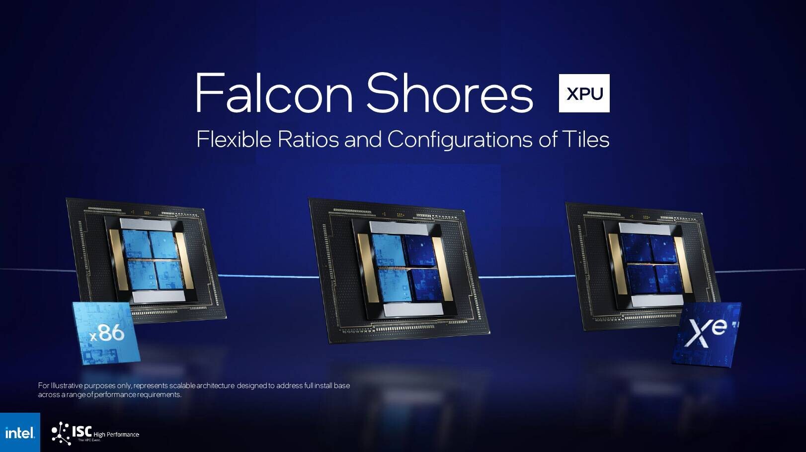
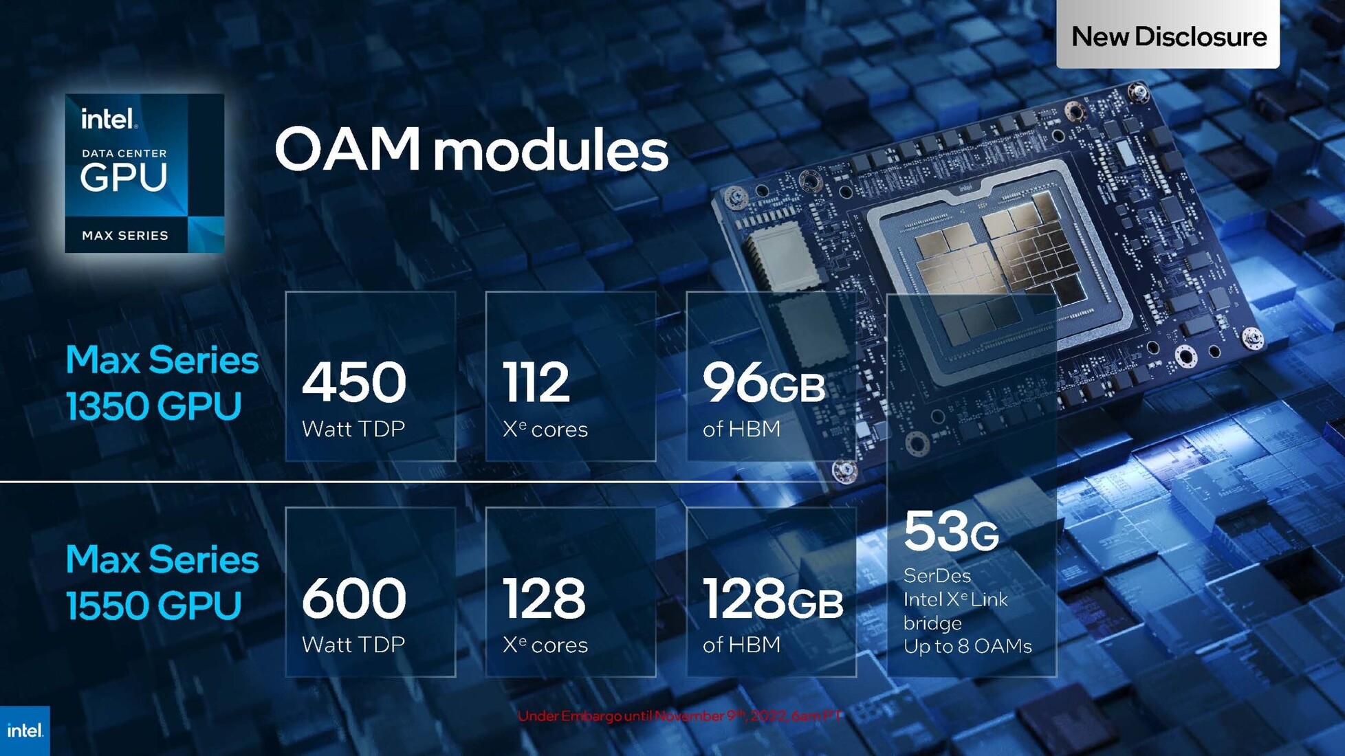
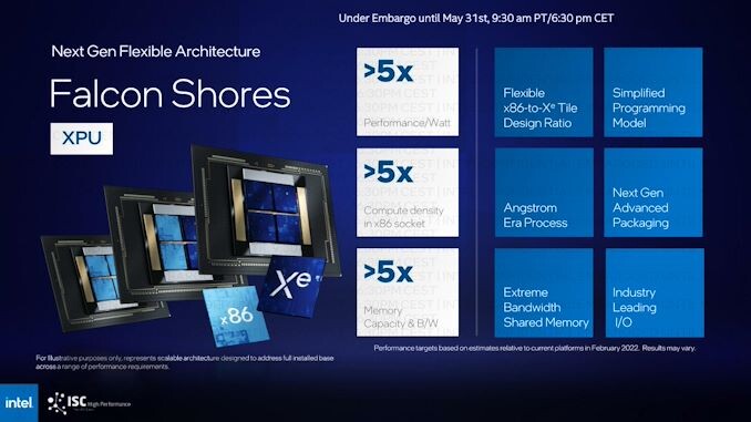
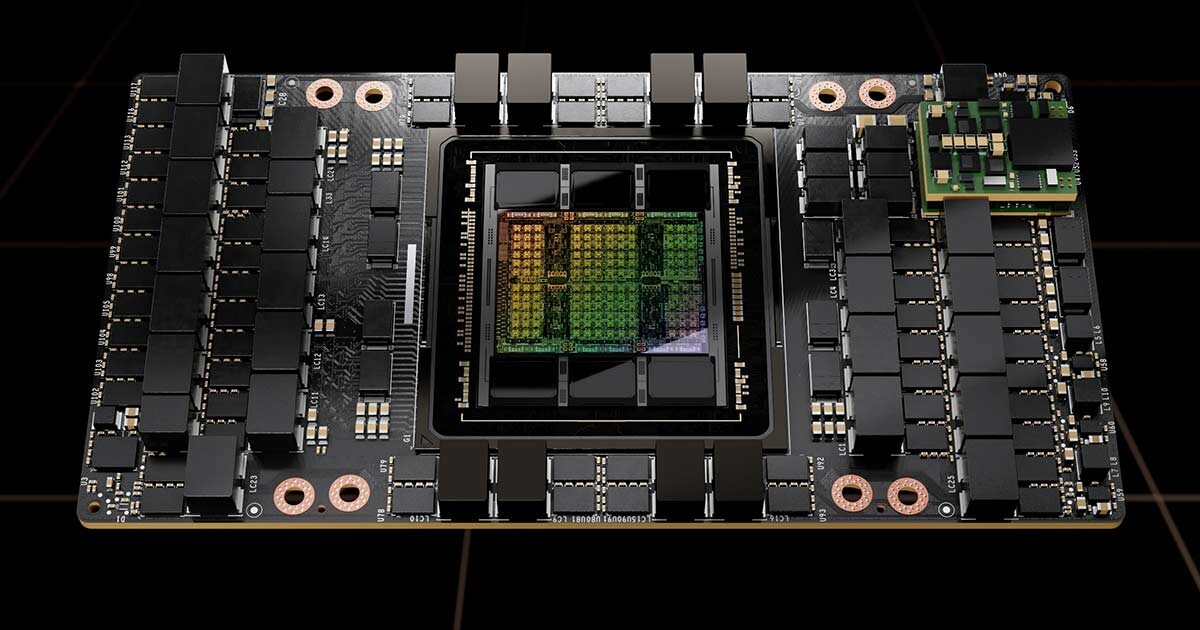
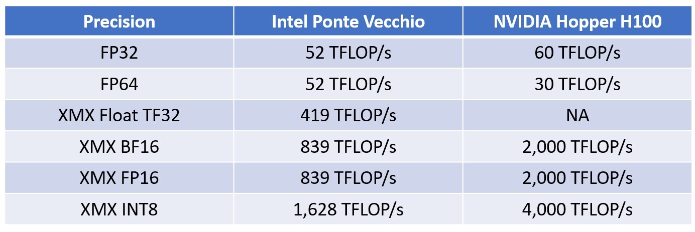
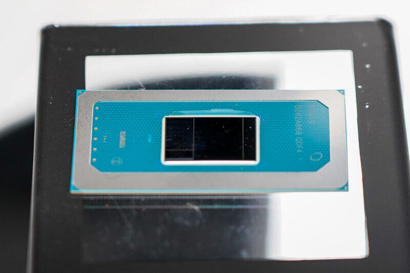
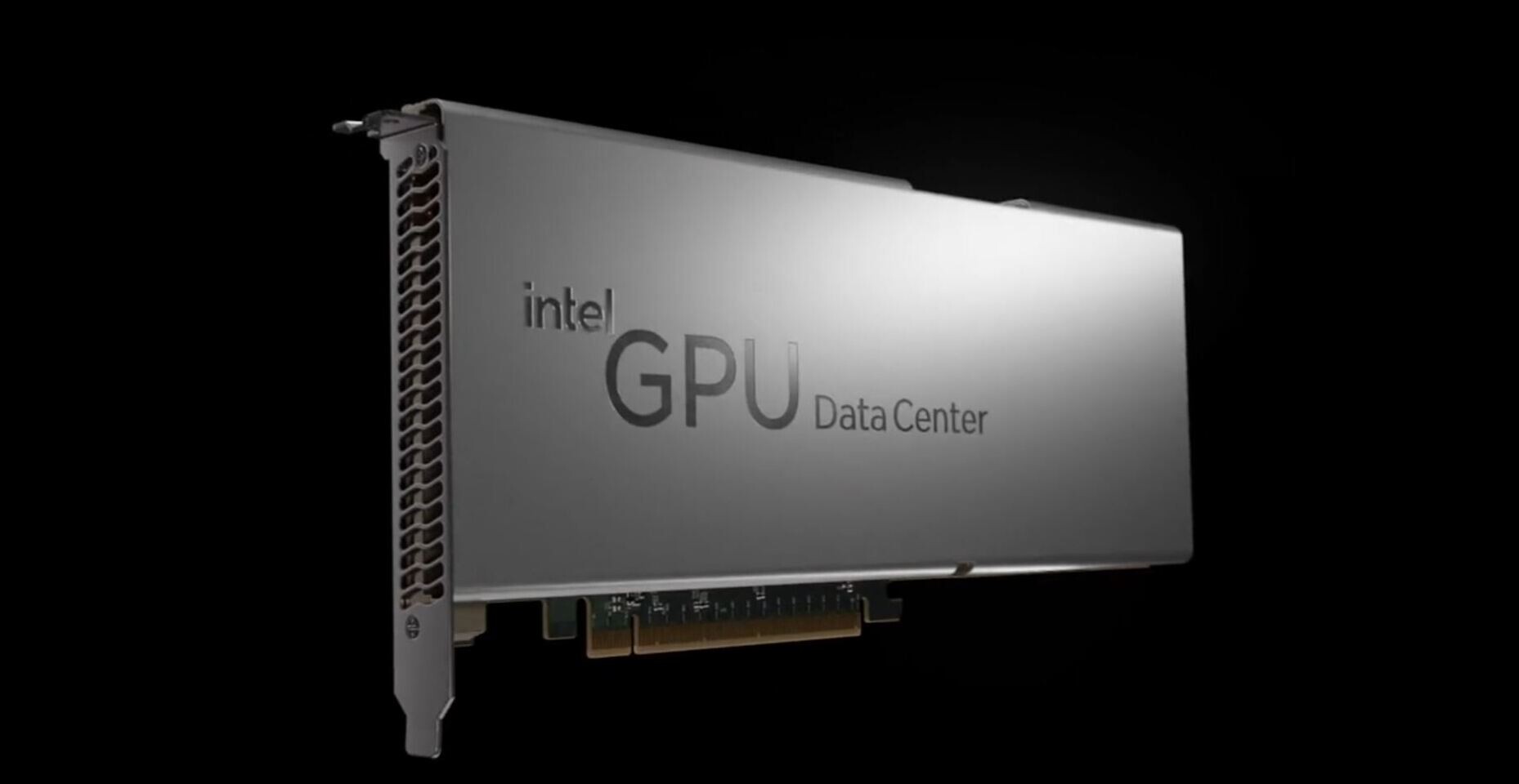
Intel retains large amounts of market-share in both the PC processor and server processor markets, however, the company's stock price has been on a downward trend for several quarters now, causing its valuation to drop to levels where any of the other big tech companies can afford to buy it out. The company spent close to $10 billion on a GPU architecture project spanning not just a contemporary graphics architecture to power the integrated graphics solutions of its PC processors, but also discrete gaming GPUs; and most importantly, an AI GPU architecture under the "Ponte Vecchio" project. Intel's Xe-HP AI GPU missed its performance targets or was too late to the market, leaving Intel with a gaping hole that it could only fill with a slew of cost-cutting measures. It doesn't help that Intel Foundry is losing its edge, and none of the logic tiles of Core Ultra "Arrow Lake" processor is made on an Intel foundry node.
Intel retains large amounts of market-share in both the PC processor and server processor markets, however, the company's stock price has been on a downward trend for several quarters now, causing its valuation to drop to levels where any of the other big tech companies can afford to buy it out. The company spent close to $10 billion on a GPU architecture project spanning not just a contemporary graphics architecture to power the integrated graphics solutions of its PC processors, but also discrete gaming GPUs; and most importantly, an AI GPU architecture under the "Ponte Vecchio" project. Intel's Xe-HP AI GPU missed its performance targets or was too late to the market, leaving Intel with a gaping hole that it could only fill with a slew of cost-cutting measures. It doesn't help that Intel Foundry is losing its edge, and none of the logic tiles of Core Ultra "Arrow Lake" processor is made on an Intel foundry node.