Non-reference AMD Radeon RX 7900 Series RDNA3 to Launch by Late-December
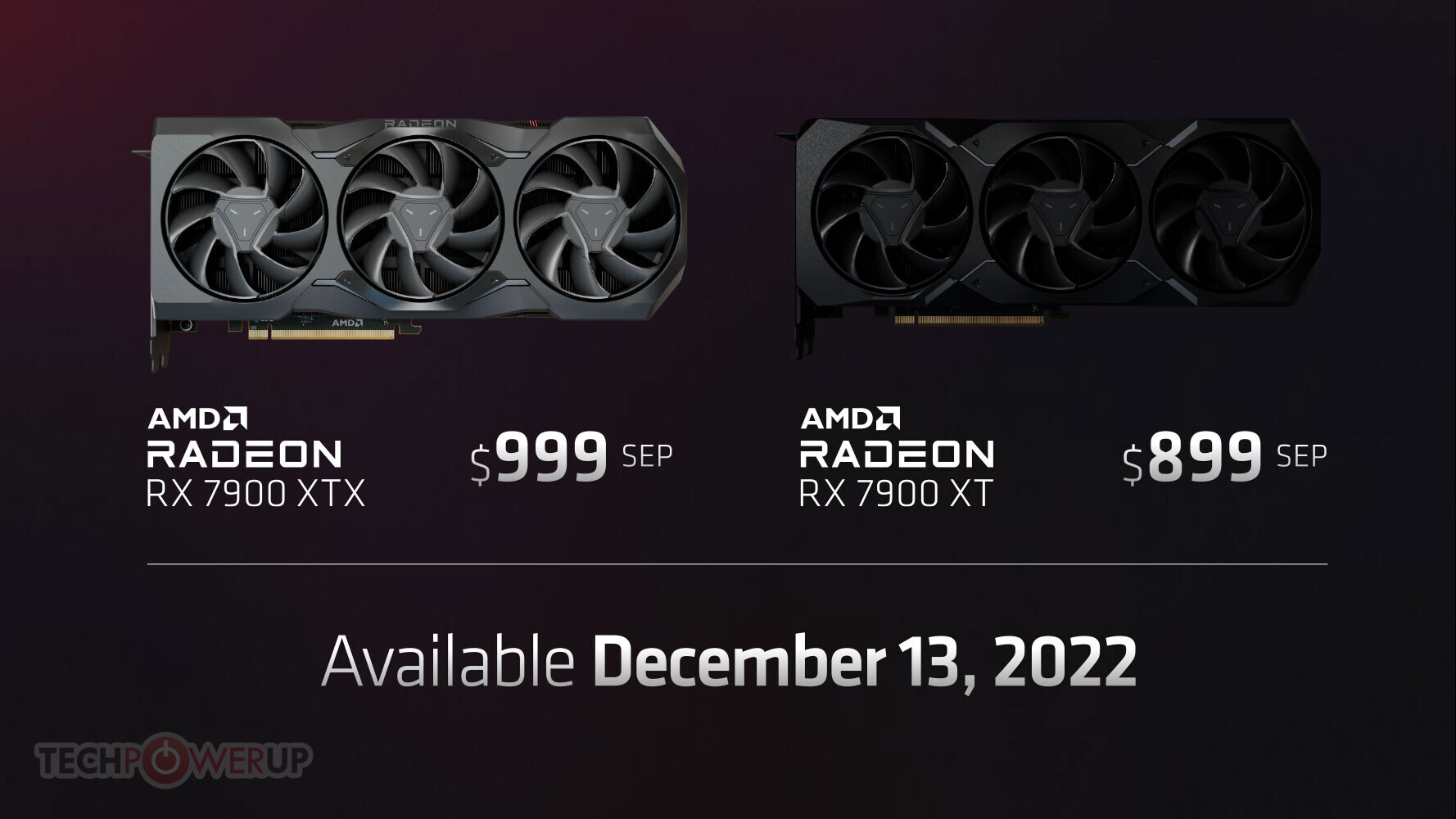
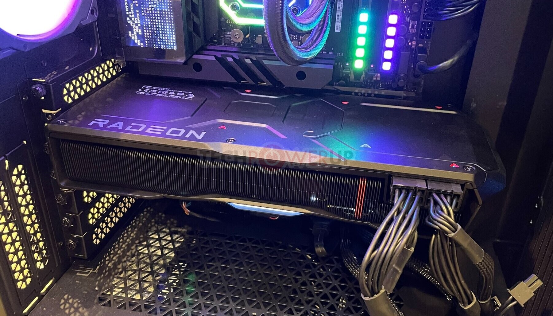
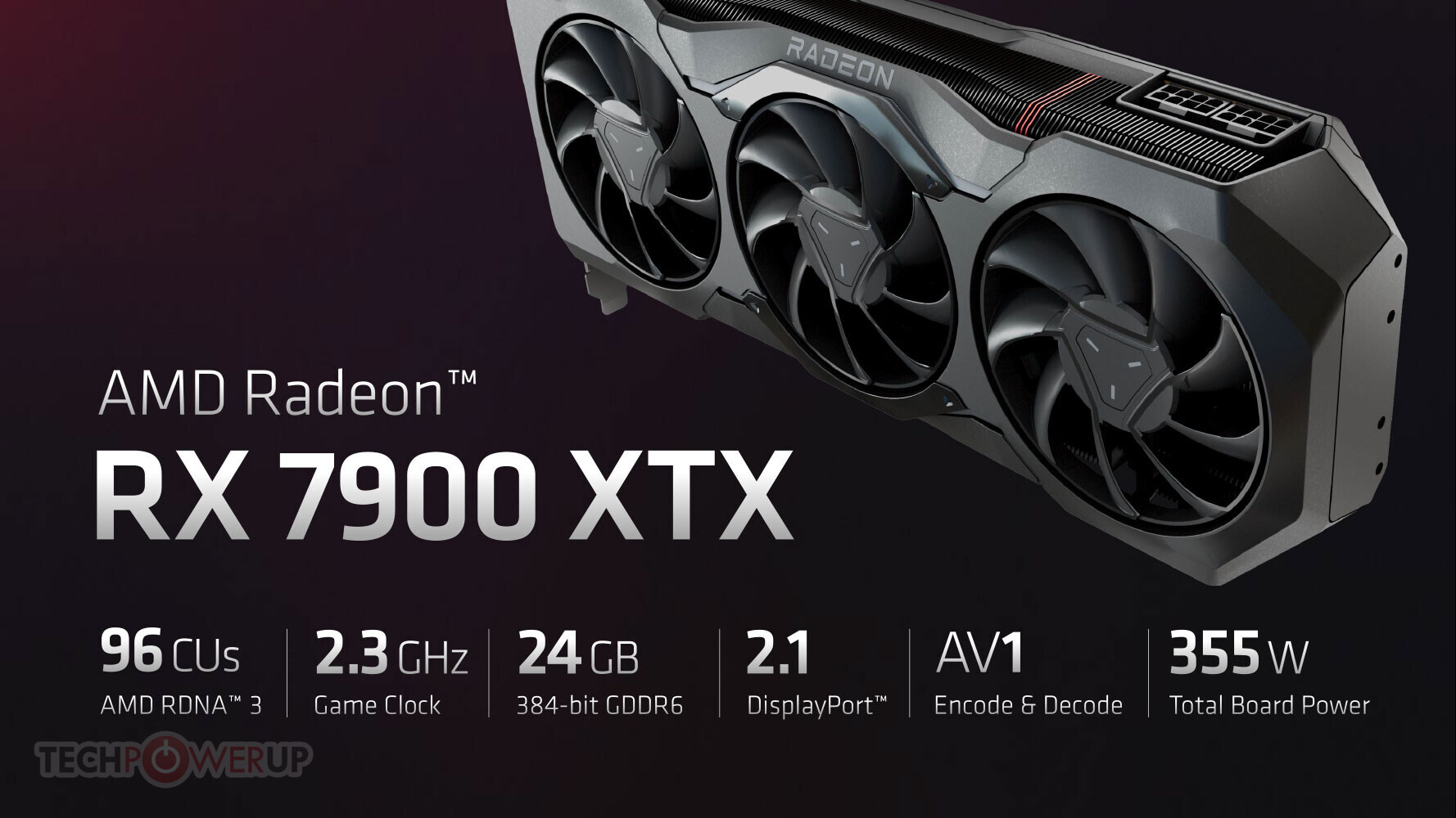
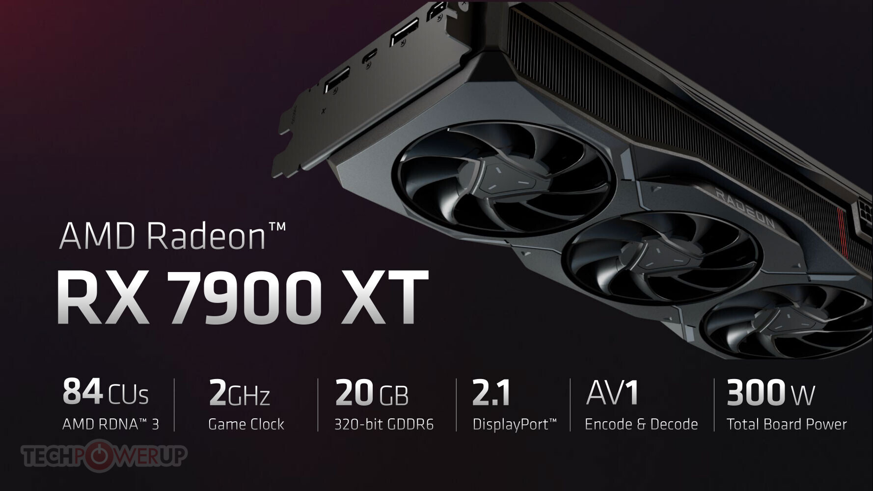
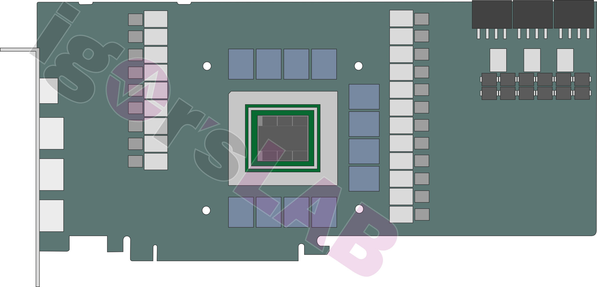
AMD Radeon RX 7900 XTX and RX 7900 XT RDNA3 graphics cards debut on December 13, 2022. This is when you will be able to buy one, at an MSRP of $999 for the RX 7900 XTX, and $899 for the RX 7900 XT. These will, however, only be reference-design MBA (made by AMD) graphics cards sold though the company's various add-in board (AIB) partners. The non-reference (custom design) RX 7900 series reportedly releases to the market 1 to 2 weeks after December 13, according to a Board Channels report seen by Wccftech.
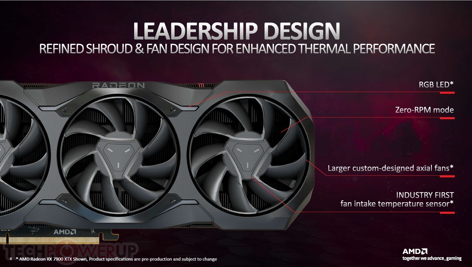
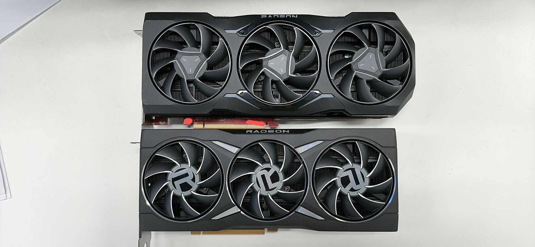
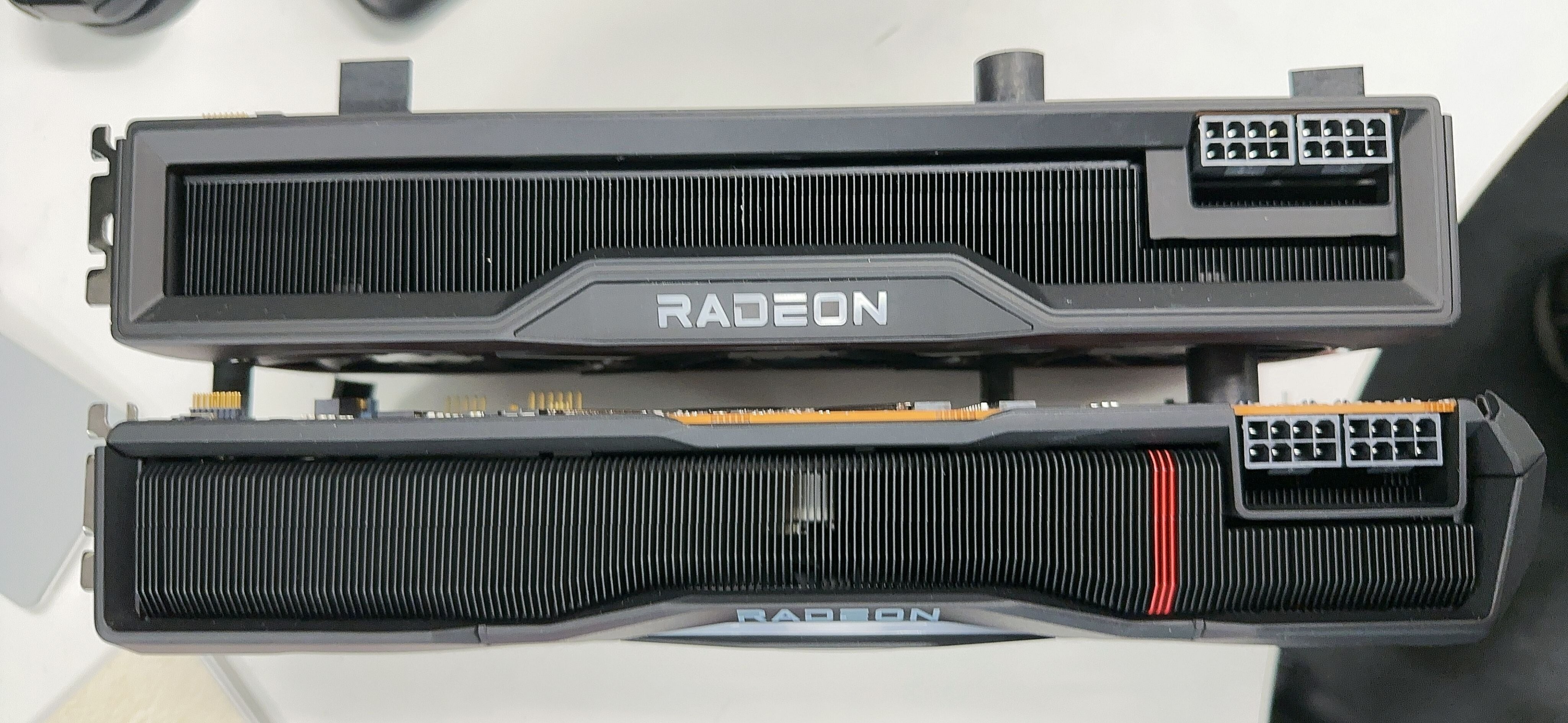
Unlike the NVIDIA Founders Edition graphics card that's sold exclusively under the NVIDIA marquee, AMD's reference-design cards are sold by its AIB partners, with minimal or nil partner branding on the cards. The after-sales support, including product warranties and other brand-specific inclusions, are handled by the AIBs themselves. Custom-design cards are those designed by the AIB partners, with customization extending to both the cooling solution and the PCB; and with some cards even featuring factory-overclocked speeds. These are the ones that could launch 1 to 2 weeks after December 13, which would put their launch anywhere between December 20 to 27 (our yikes go out to reviewers).
Unlike the NVIDIA Founders Edition graphics card that's sold exclusively under the NVIDIA marquee, AMD's reference-design cards are sold by its AIB partners, with minimal or nil partner branding on the cards. The after-sales support, including product warranties and other brand-specific inclusions, are handled by the AIBs themselves. Custom-design cards are those designed by the AIB partners, with customization extending to both the cooling solution and the PCB; and with some cards even featuring factory-overclocked speeds. These are the ones that could launch 1 to 2 weeks after December 13, which would put their launch anywhere between December 20 to 27 (our yikes go out to reviewers).