NVIDIA Shares Details About Ampere Founders Edition Cooling & Power Design - 12-pin Confirmed
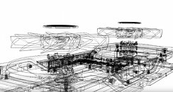
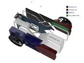
NVIDIA today shared the design philosophy behind the cooling solution of its next-generation GeForce "Ampere" RTX 3080 / 3090 graphics cards, which we'll hopefully learn more about on September 1, when NVIDIA has scheduled a GeForce Special Event. Part of the new video presentation shows the evolution of NVIDIA's cooling solutions over the years. NVIDIA explains the four pillars behind the design, stressing that thermals are at the heart of its innovation, and that the company looks to explore new ways to use air-cooling more effectively to cool graphics cards. To this effect, the cooling solution of the upcoming GeForce Ampere Founders Edition graphics cards features an airflow-optimized design focused on ensuring the most effective way to take in fresh air, transfer heat to it, and exhaust the warm air in the most optimal manner.
The next pillar of NVIDIA's cooling technology innovation is mechanical structure, to minimize the structural components of the cooler without compromising on strength. The new Founder Edition cooler introduces a new low profile leaf spring that leaves more room for a back cover. Next up is reducing the electrical clutter, with the introduction of a new 12-pin power connector that is more compact, consolidates cabling, and yet does not affect the card's power delivery capability. The last pillar is product design, which puts NVIDIA's innovations together in an airy new industrial design. The video presentation includes commentary from NVIDIA's product design engineers who explain the art and science behind the next GeForce. NVIDIA is expected to tell us more about the next generation GeForce Ampere at a Special Event on September 1.
The next pillar of NVIDIA's cooling technology innovation is mechanical structure, to minimize the structural components of the cooler without compromising on strength. The new Founder Edition cooler introduces a new low profile leaf spring that leaves more room for a back cover. Next up is reducing the electrical clutter, with the introduction of a new 12-pin power connector that is more compact, consolidates cabling, and yet does not affect the card's power delivery capability. The last pillar is product design, which puts NVIDIA's innovations together in an airy new industrial design. The video presentation includes commentary from NVIDIA's product design engineers who explain the art and science behind the next GeForce. NVIDIA is expected to tell us more about the next generation GeForce Ampere at a Special Event on September 1.

