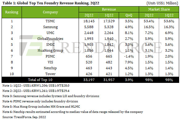
2Q22 Output Value Growth at Top 10 Foundries Falls to 3.9% QoQ, Says TrendForce
According to TrendForce research, due to steady weakening of overall demand for consumer electronics, inventory pressure has increased among downstream distributors and brands. Although there are still sporadic shortages of specific components, the curtain has officially fallen on a two-year wave of shortages in general, and brands have gradually suspended stocking in response to changes in market conditions. However, stable demand for automotive and industrial equipment is key to supporting the ongoing growth of foundry output value. At the same time, since the creation of a marginal amount of new capacity in 2Q22 led to growth in wafer shipments and a price hike for certain wafers, this drove output value among top ten foundries to reach US$33.20 billion in 2Q22. Quarterly growth fell to 3.9% on a weakening consumer market.
A prelude to inventory correction was officially revealed in 3Q22. In addition to intensifying severity in the initial wave of order slashing for LDDI/TDDI, and TV SoC, diminishing order volume also extended to non-Apple smartphone APs and peripheral IC PMIC, CIS, and consumer electronics PMICs, and mid-to-low-end MCUs, posing a challenge for foundry capacity utilization. However, the launch of the new iPhone in 3Q22 is expected to prop up a certain amount of stocking momentum for the sluggish market. Therefore, top ten foundry revenue in 3Q22 is expected to maintain a growth trend driven by high-priced processes and quarterly growth rate is expected to be slightly higher than in 2Q22.
A prelude to inventory correction was officially revealed in 3Q22. In addition to intensifying severity in the initial wave of order slashing for LDDI/TDDI, and TV SoC, diminishing order volume also extended to non-Apple smartphone APs and peripheral IC PMIC, CIS, and consumer electronics PMICs, and mid-to-low-end MCUs, posing a challenge for foundry capacity utilization. However, the launch of the new iPhone in 3Q22 is expected to prop up a certain amount of stocking momentum for the sluggish market. Therefore, top ten foundry revenue in 3Q22 is expected to maintain a growth trend driven by high-priced processes and quarterly growth rate is expected to be slightly higher than in 2Q22.