News Posts matching #Wafer

Return to Keyword Browsing

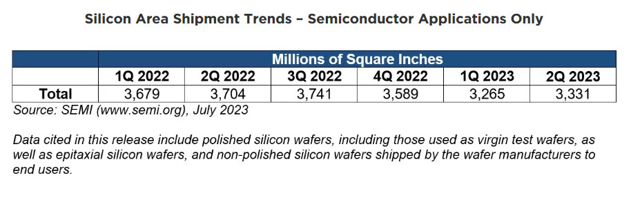
Samsung Aims for 1,000-Layer NAND by 2030, Begins Wafer Bonding at 400 Layers

Samsung aims to create 1,000-layer NAND by 2030 relying on its new "multi-BV" NAND design. The Bell reports that this plan involves stacking four wafers to overcome structural limits. Wafer bonding technology plays a crucial role in this progress and Samsung intends to use it to break the 1,000-layer barrier. Samsung Electronics DS division CTO, Song Jae-hyuk, pointed out that wafer bonding allows separate production of peripheral and cell wafers before joining them into one semiconductor. The Bell says this technology will likely appear first in Samsung's 10th-gen NAND (V10), while industry experts think a single wafer can hold about 500 NAND layers when implementing only cell structures. In the past, Samsung has used the COP (Cell on Peripheral) technique, a method that places the peripheral circuit on one wafer, with NAND cells stacked on top. However, as NAND layers grow, the lower peripheral parts face more pressure potentially affecting reliability.

Samsung's plan involves working with China's YMTC, which should offer a hybrid bonding patent for V10 NAND. ZDNet reports that the South Korean tech company will start making its V10 NAND in large quantities in the second half of 2025, with about 420-430 layers. Besides wafer bonding, Samsung adds other technologies to its NAND plan. The Bell points out that cold etching using molybdenum, and other new ideas will start with 400-layer NAND and play a key part in growing to 1,000 layers. Samsung isn't alone in trying to create ultra-high-layer NAND products. Japan's Kioxia also wants to reach this goal through its "multi-stack CBA" (CMOS Bonded to Array) technology. The company's plan is even bolder hoping to sell 1,000-layer 3D NAND by 2027.

Intel's High-NA EUV Machines Already Processed 30,000 Wafers, More to Come with 14A Node

Intel has successfully deployed two advanced ASML High-NA Twinscan EXE:5000 EUV lithography systems at its D1 development facility near Hillsboro, Oregon, processing approximately 30,000 wafers in a single quarter. The High-NA EUV systems, each reportedly valued at $380 million, represent a substantial improvement over previous lithography tools, achieving resolution down to 8 nm with a single exposure compared to the 13.5 nm resolution of current Low-NA systems. Early operational data indicates these machines are approximately twice as reliable as previous EUV generations, addressing reliability challenges that previously hampered Intel's manufacturing progress. The ability to accomplish with a single exposure what previously required three exposures and approximately 40 processing steps has been reduced to just "single digit" processing steps.

Intel has historically been an early adopter of high-NA EUV lithography, a much more aggressive strategy than its competitors like TSMC, which manufactures its advanced silicon using low-NA EUV tools. The company plans to utilize these systems for its upcoming 14A chip manufacturing process, though no specific mass production date has been announced. While ASML classifies these Twinscan EXE:5000 systems as pre-production tools not designed for high-volume manufacturing, Intel's extensive wafer processing is more of a test bed. The early adoption provides Intel with valuable development opportunities across various High-NA EUV manufacturing aspects, including photomask glass, pellicles, and specialized chemicals that could establish future industry standards. Intel's current 18A node is utilizing Low-NA lithography tools, where Intel is only exploring High-NA with it for testing, before moving on to 14A high-volume manufacturing with High-NA EUV.

TSMC 2 nm Wafer Output Projected to Reach 80,000 Units Per Month, by End of 2025

Earlier in the year, we heard about TSMC being ahead of the game with its speculated trial production run of cutting-edge 2 nm (N2) silicon. Taiwan's premier foundry company is reportedly prepping its Baoshan and Kaohsiung plants for full-on manufacturing of next-gen chips. The latest insider whispers propose that TSMC is making "rapid" progress on the 2 nm (N2) front, as company engineers have moved onto an "intensive" trial production phase. Taiwan's Economic Daily News has picked up on compelling projections from industry moles; the Hsinchu Baoshan facility's current monthly production capacity is (allegedly) around 5000 to 10,000 2 nm wafers. The other 2 nm-specialist site—Kaohsiung—has reportedly moved into a small-scale appraisal phase.

TSMC declined to comment on recently leaked data points, but they released a general statement (to UDN), emphasizing that: "(our) 2 nm process technology is progressing well and will go into mass production as scheduled in the second half of this year." The Baoshan plant could ramp up to 25,000 2 nm wafers per month, once it moves into a mass production phase. Combined with the same estimated output from its sister site (Kaohsiung), insiders reckon that the combined total could reach 50,000 units per month. Following a predicted successful "second phase" transition, TSMC's most advanced facilities have a "chance" to pump out 80,000 2 nm parts (combined total). The latest murmurs suggest that this milestone could be achieved by the end of 2025. Industry watchdogs believe that Apple will have first access dibs on TSMC's upcoming cutting-edge offerings.

Global Semiconductor Manufacturing Industry Reports Solid Q4 2024 Results

The global semiconductor manufacturing industry closed 2024 with strong fourth quarter results and solid year-on-year (YoY) growth across most of the key industry segments, SEMI announced today in its Q4 2024 publication of the Semiconductor Manufacturing Monitor (SMM) Report, prepared in partnership with TechInsights. The industry outlook is cautiously optimistic at the start of 2025 as seasonality and macroeconomic uncertainty may impede near-term growth despite momentum from strong investments related to AI applications.

After declining in the first half of 2024, electronics sales bounced back later in the year resulting in a 2% annual increase. Electronics sales grew 4% YoY in Q4 2024 and are expected to see a 1% YoY increase in Q1 2025 impacted by seasonality. Integrated circuit (IC) sales rose by 29% YoY in Q4 2024 and continued growth is expected in Q1 2025 with a 23% increase YoY as AI-fueled demand continues boosting shipments of high-performance computing (HPC) and datacenter memory chips.

Around 20,000 TSMC Wafers Reported Damaged by Earthquake

Earlier this week, Taiwan experienced a magnitude 6.4 earthquake—this seismic event interrupted manufacturing activities at several TSMC chip-making facilities. As a precaution, foundry employees in both Central and Southern Taiwan were evacuated. Production resumed fairly quickly following inspections of crucial infrastructure—no major damage to facilities or equipment was noted. The latest reports suggest that a relatively minor number of TSMC wafers have been affected by the recent quake, while some recalibration of instrumentation is required to get things back on track.

Inside sources reckon that up to 20,000 wafers (possibly 10,000 at a minimum) could be scrapped—assessments are reportedly still underway, but a small proportion of client shipments could be disrupted. News articles point to this total being spread across three affected locations. Fab 18 is a key 3 nm production hub—situated in Taiwan's Southern Science Park, Tainan's Fab 14 specializes in 4 nm and 5 nm processes, and Fab 8 (Hsinchu) takes care of 200 nm. Industry experts believe that TSMC will bounce back quickly, and that the damaged wafer count represents a minor dent in the proverbial armor—on a good day, manufacturing output can reach up to 37,000 units.

GlobalWafers Awarded $406M via U.S. CHIPS Act to Boost 300mm Wafer Supply

The U.S. Department of Commerce will award GlobalWafers America and MEMC, LLC, U.S. subsidiaries of Taiwan-based GlobalWafers Co., Ltd., up to $406 million in direct funding under the CHIPS Incentives Program's Funding Opportunity for Commercial Fabrication Facilities.

The award will support planned investments of $4 billion in advanced semiconductor wafer manufacturing facilities in Sherman, Texas and St. Peters, Missouri. The Department will disburse the funds based on GWA's and MEMC's completion of project milestones over a multi-year timeframe.

Global Total Semiconductor Equipment Sales Forecast to Reach a Record of $139 Billion in 2026

Global sales of total semiconductor manufacturing equipment by original equipment manufacturers (OEMs) are forecast to set a new industry record, reaching $113 billion in 2024, growing 6.5% year-on-year, SEMI announced today in its Year-End Total Semiconductor Equipment Forecast - OEM Perspective at SEMICON Japan 2024. Semiconductor manufacturing equipment growth is expected to continue in the following years, reaching new records of $121 billion in 2025 and $139 billion in 2026, supported by both the front-end and back-end segments.

"Three consecutive years of projected growth in investments in semiconductor manufacturing reflect the vital role our industry plays in underpinning the global economy and advancing technology innovation," said Ajit Manocha, SEMI president and CEO. "Since our July 2024 forecast, the outlook for 2024 semiconductor equipment sales has brightened, especially with stronger-than-expected investments from China and in AI-related sectors. Together with our forecast extension through 2026, it highlights the robust growth drivers across segments, applications, and regions."

Intel Appoints Semiconductor Leaders Eric Meurice and Steve Sanghi to Board of Directors

Intel Corporation today announced that Eric Meurice, former president, chief executive officer and chairman of ASML Holding N.V., and Steve Sanghi, chairman and interim chief executive officer of Microchip Technology Inc., have been appointed to Intel's board of directors, effective immediately. Both will serve as independent directors.

"Eric and Steve are highly respected leaders in the semiconductor industry whose deep technical expertise, executive experience and operational rigor make them great additions to the Intel board," said Frank D. Yeary, interim executive chair of the Intel board. "As successful CEOs with proven track records of creating shareholder value, they will bring valuable perspectives to the board as the company delivers on its priorities for customers in Intel Products and Intel Foundry, while driving greater efficiency and improving profitability."

Worldwide Silicon Wafer Shipments Increase 6% in Q3 2024, SEMI Reports

Worldwide silicon wafer shipments increased 5.9% quarter-over-quarter to 3,214 million square inches (MSI) in the third quarter of 2024 and registered 6.8% growth from the 3,010 million square inches recorded during the same quarter last year, the SEMI Silicon Manufacturers Group (SMG) reported in its quarterly analysis of the silicon wafer industry.

"The third quarter wafer shipment results continued the upward trend which started in the second quarter of this year," said Lee Chungwei (李崇偉), Chairman of SEMI SMG and Vice President and Chief Auditor at GlobalWafers. "Inventory levels have declined throughout the supply chain but generally remain high. Demand for advanced wafers used for AI continues to be strong. However, the silicon wafer demand for automotive and industrial uses continues to be muted, while the demand for silicon used for handset and other consumer products has seen some areas of improvement. As a result, 2025 is likely to continue upward trends, but total shipments are not yet expected to return to the peak levels of 2022."

Infineon Unveils the World's Thinnest Silicon Power Wafer

After announcing the world's first 300-millimeter gallium nitride (GaN) power wafer and opening the world's largest 200-millimeter silicon carbide (SiC) power fab in Kulim, Malaysia, Infineon Technologies AG has unveiled the next milestone in semiconductor manufacturing technology. Infineon has reached a breakthrough in handling and processing the thinnest silicon power wafers ever manufactured, with a thickness of only 20 micrometers and a diameter of 300 millimeters, in a high-scale semiconductor fab. The ultra-thin silicon wafers are only a quarter as thick as a human hair and half as thick as current state-of-the-art wafers of 40-60 micrometers.

"The world's thinnest silicon wafer is proof of our dedication to deliver outstanding customer value by pushing the technical boundaries of power semiconductor technology," said Jochen Hanebeck, CEO at Infineon Technologies. "Infineon's breakthrough in ultra-thin wafer technology marks a significant step forward in energy-efficient power solutions and helps us leverage the full potential of the global trends decarbonization and digitalization. With this technological masterpiece, we are solidifying our position as the industry's innovation leader by mastering all three relevant semiconductor materials: Si, SiC and GaN."

Global Silicon Wafer Shipments to Remain Soft in 2024 Before Strong Expected Rebound in 2025, SEMI Reports

Global shipments of silicon wafers are projected to decline 2% in 2024 to 12,174 million square inches (MSI) with a strong rebound of 10% delayed until 2025 to reach 13,328 MSI as wafer demand continues to recover from the downcycle, SEMI reported today in its annual silicon shipment forecast.

Strong silicon wafer shipment growth is expected to continue through 2027 to meet increasing demand related to AI and advanced processing, driving improved fab utilization rate for global semiconductor production capacity. Moreover, new applications in advanced packaging and high-bandwidth memory (HBM) production, which require additional wafers, are contributing to the rising need for silicon wafers. Such applications include temporary or permanent carrier wafers, interposers, device separation into chiplets, and memory/logic array separation.

Amkor and TSMC to Expand Partnership and Collaborate on Advanced Packaging in Arizona

Amkor Technology, Inc. and TSMC announced today that the two companies have signed a memorandum of understanding to collaborate and bring advanced packaging and test capabilities to Arizona, further expanding the region's semiconductor ecosystem.

Amkor and TSMC have been closely collaborating to deliver high volume, leading-edge technologies for advanced packaging and testing of semiconductors to support critical markets such as high-performance computing and communications. Under the agreement, TSMC will contract turnkey advanced packaging and test services from Amkor in their planned facility in Peoria, Arizona. TSMC will leverage these services to support its customers, particularly those using TSMC's advanced wafer fabrication facilities in Phoenix. The close collaboration and proximity of TSMC's front-end fab and Amkor's back-end facility will accelerate overall product cycle times.

Infineon Announces World's First 300 mm Power Gallium Nitride (GaN) Technology

Infineon Technologies AG today announced that the company has succeeded in developing the world's first 300 mm power gallium nitride (GaN) wafer technology. Infineon is the first company in the world to master this groundbreaking technology in an existing and scalable high-volume manufacturing environment. The breakthrough will help substantially drive the market for GaN-based power semiconductors. Chip production on 300 mm wafers is technologically more advanced and significantly more efficient compared to 200 mm wafers, since the bigger wafer diameter offers 2.3 times more chips per wafer.

GaN-based power semiconductors find fast adoption in industrial, automotive, and consumer, computing & communication applications, including power supplies for AI systems, solar inverters, chargers and adapters, and motor-control systems. State-of-the art GaN manufacturing processes lead to improved device performance resulting in benefits in end customers' applications as it enables efficiency performance, smaller size, lighter weight, and lower overall cost. Furthermore, 300 mm manufacturing ensures superior customer supply stability through scalability.

TSMC to Raise Wafer Prices by 10% in 2025, Customers Seemingly Agree

Taiwanese semiconductor giant TSMC is reportedly planning to increase its wafer prices by up to 10% in 2025, according to a Morgan Stanley note cited by investor Eric Jhonsa. The move comes as demand for cutting-edge processors in smartphones, PCs, AI accelerators, and HPC continues to surge. Industry insiders reveal that TSMC's state-of-the-art 4 nm and 5 nm nodes, used for AI and HPC customers such as AMD, NVIDIA, and Intel, could see up to 10% price hikes. This increase would push the cost of 4 nm-class wafers from $18,000 to approximately $20,000, representing a significant 25% rise since early 2021 for some clients and an 11% rise from the last price hike. Talks about price hikes with major smartphone manufacturers like Apple have proven challenging, but there are indications that modest price increases are being accepted across the industry. Morgan Stanley analysts project a 4% average selling price increase for 3 nm wafers in 2025, which are currently priced at $20,000 or more per wafer.

Mature nodes like 16 nm are unlikely to see price increases due to sufficient capacity. However, TSMC is signaling potential shortages in leading-edge capacity to encourage customers to secure their allocations. Adding to the industry's challenges, advanced chip-on-wafer-on-substrate (CoWoS) packaging prices are expected to rise by 20% over the next two years, following previous increases in 2022 and 2023. TSMC aims to boost its gross margin to 53-54% by 2025, anticipating that customers will absorb these additional costs. The impact of these price hikes on end-user products remains uncertain. Competing foundries like Intel and Samsung may seize this opportunity to offer more competitive pricing, potentially prompting some chip designers to consider alternative manufacturing options. Additionally, TSMC's customers could reportedly be unable to secure their capacity allocation without "appreciating TSMC's value."

TSMC Begins Experimenting with Rectangular Panel-Like Chip Packaging

TSMC is working on a new advanced chip packaging technology that uses rectangular panel-like substrates instead of the traditional circular wafers, according to a Nikkei report citing sources. This new approach would allow more chips to be placed on a single substrate. TSMC is reportedly experimenting with rectangular substrates measuring 515 mm by 510 mm, providing more than three times the usable area compared to current 12-inch wafers. Using a rectangular-shaped wafer can potentially eliminate more of the incomplete chips found on the edges of current circular ones. While this may sound simple, it would actually require a radical change to the entire manufacturing process.

While the research is still in its early stages and may take several years to reach mass production, it represents a major technological shift for TSMC. The company has responded to Nikkei's inquiry by stating that they are closely monitoring advancements in advanced packaging technologies, including panel-level packaging. This development could potentially give TSMC an edge in meeting future chip demands, however, Intel and Samsung are also testing this new approach.

TSMC Celebrates 30th North America Technology Symposium with Innovations Powering AI with Silicon Leadership

TSMC today unveiled its newest semiconductor process, advanced packaging, and 3D IC technologies for powering the next generation of AI innovations with silicon leadership at the Company's 2024 North America Technology Symposium. TSMC debuted the TSMC A16 technology, featuring leading nanosheet transistors with innovative backside power rail solution for production in 2026, bringing greatly improved logic density and performance. TSMC also introduced its System-on-Wafer (TSMC-SoW) technology, an innovative solution to bring revolutionary performance to the wafer level in addressing the future AI requirements for hyperscaler datacenters.

This year marks the 30th anniversary of TSMC's North America Technology Symposium, and more than 2,000 attended the event, growing from less than 100 attendees 30 years ago. The North America Technology Symposium in Santa Clara, California kicks off TSMC Technology Symposiums around the world in the coming months. The symposium also features an "Innovation Zone," designed to highlight the technology achievements of our emerging start-up customers.

Arizona State University and Deca Technologies to Pioneer North America's First R&D Center for Advanced Fan-Out Wafer-Level Packaging

Arizona State University (ASU) and Deca Technologies (Deca), a premier provider of advanced wafer- and panel-level packaging technology, today announced a groundbreaking collaboration to create North America's first fan-out wafer-level packaging (FOWLP) research and development center.

The new Center for Advanced Wafer-Level Packaging Applications and Development is set to catalyze innovation in the United States, expanding domestic semiconductor manufacturing capabilities and driving advancements in cutting-edge fields such as artificial intelligence, machine learning, automotive electronics and high-performance computing.

Cerebras & G42 Break Ground on Condor Galaxy 3 - an 8 exaFLOPs AI Supercomputer

Cerebras Systems, the pioneer in accelerating generative AI, and G42, the Abu Dhabi-based leading technology holding group, today announced the build of Condor Galaxy 3 (CG-3), the third cluster of their constellation of AI supercomputers, the Condor Galaxy. Featuring 64 of Cerebras' newly announced CS-3 systems - all powered by the industry's fastest AI chip, the Wafer-Scale Engine 3 (WSE-3) - Condor Galaxy 3 will deliver 8 exaFLOPs of AI with 58 million AI-optimized cores. The Cerebras and G42 strategic partnership already delivered 8 exaFLOPs of AI supercomputing performance via Condor Galaxy 1 and Condor Galaxy 2, each amongst the largest AI supercomputers in the world. Located in Dallas, Texas, Condor Galaxy 3 brings the current total of the Condor Galaxy network to 16 exaFLOPs.

"With Condor Galaxy 3, we continue to achieve our joint vision of transforming the worldwide inventory of AI compute through the development of the world's largest and fastest AI supercomputers," said Kiril Evtimov, Group CTO of G42. "The existing Condor Galaxy network has trained some of the leading open-source models in the industry, with tens of thousands of downloads. By doubling the capacity to 16exaFLOPs, we look forward to seeing the next wave of innovation Condor Galaxy supercomputers can enable." At the heart of Condor Galaxy 3 are 64 Cerebras CS-3 Systems. Each CS-3 is powered by the new 4 trillion transistor, 900,000 AI core WSE-3. Manufactured at TSMC at the 5-nanometer node, the WSE-3 delivers twice the performance at the same power and for the same price as the previous generation part. Purpose built for training the industry's largest AI models, WSE-3 delivers an astounding 125 petaflops of peak AI performance per chip.

Report: Global Semiconductor Capacity Projected to Reach Record High 30 Million Wafers Per Month in 2024

Global semiconductor capacity is expected to increase 6.4% in 2024 to top the 30 million *wafers per month (wpm) mark for the first time after rising 5.5% to 29.6 wpm in 2023, SEMI announced today in its latest quarterly World Fab Forecast report.

The 2024 growth will be driven by capacity increases in leading-edge logic and foundry, applications including generative AI and high-performance computing (HPC), and the recovery in end-demand for chips. The capacity expansion slowed in 2023 due to softening semiconductor market demand and the resulting inventory correction.

Semiconductor Market to Grow 20.2% in 2024 to $633 Billion, According to IDC

International Data Corporation (IDC) has upgraded its Semiconductor Market Outlook by calling a bottom and return to growth that accelerates next year. IDC raised its September 2023 revenue outlook from $518.8 billion to $526.5 billion in a new forecast. Revenue expectations for 2024 were also raised from $625.9 billion to $632.8 billion as IDC believes the U.S. market will remain resilient from a demand standpoint and China will begin recovering by the second half of 2024 (2H24).

IDC sees better semiconductor growth visibility as the long inventory correction subsides in two of the largest market segments: PCs and smartphones. Automotive and Industrials elevated inventory levels are expected to return to normal levels in 2H24 as electrification continues to drive semiconductor content over the next decade. Technology and large flagship product introductions will drive more semiconductor content and value across market segments in 2024 through 2026, including the introduction of AI PCs and AI Smartphones next year and a much-needed improvement in memory ASPs and DRAM bit volume.

Texas Instruments Breaks Ground on New 300-mm Semiconductor Wafer Fabrication Plant in Utah

Texas Instruments (TI) today broke ground on its new 300-mm semiconductor wafer fabrication plant (or "fab") in Lehi, Utah. Joined by Utah Governor Spencer Cox, state and local elected officials, as well as community leaders, TI President and Chief Executive Officer Haviv Ilan celebrated the first steps toward construction of the new fab, LFAB2, which will connect to the company's existing 300-mm wafer fab in Lehi. Once completed, TI's two Utah fabs will manufacture tens of millions of analog and embedded processing chips every day at full production.

"Today we take an important step in our company's journey to expand our manufacturing footprint in Utah. This new fab is part of our long-term, 300-mm manufacturing roadmap to build the capacity our customers will need for decades to come," said Ilan. "At TI, our passion is to create a better world by making electronics more affordable through semiconductors. We are proud to be a growing member of the Utah community, and to manufacture analog and embedded processing semiconductors that are vital for nearly every type of electronic system today."

TSMC Ramps Up CoWoS Advanced Packaging Production to Meet Soaring AI Chip Demand

The burgeoning AI market is significantly impacting TSMC's CoWoS (Chip on Wafer on Substrate) advanced packaging production capacity, causing it to overflow due to high demand from major companies like NVIDIA, AMD, and Amazon. To accommodate this, TSMC is in the process of expanding its production capacity by acquiring additional CoWoS machines from equipment manufacturers like Xinyun, Wanrun, Hongsu, Titanium, and Qunyi. These expansions are expected to be operational in the first half of the next year, leading to an increased monthly production capacity, potentially close to 30,000 pieces, enabling TSMC to cater to more AI-related orders. These endeavors to increase capacity are in response to the amplified demand for AI chips from their applications in various domains, including autonomous vehicles and smart factories.

Despite TSMC's active steps to enlarge its CoWoS advanced packaging production, the overwhelming client demand is driving the company to place additional orders with equipment suppliers. It has been indicated that NVIDIA is currently TSMC's largest CoWoS advanced packaging customer, accounting for 60% of its production capacity. Due to the surge in demand, companies like AMD, Amazon, and Broadcom are also placing urgent orders, leading to a substantial increase in TSMC's advanced process capacity utilization. The overall situation indicates a thriving scenario for equipment manufacturers with clear visibility of orders extending into the following year, even as they navigate the challenges of fulfilling the rapidly growing and immediate demand in the AI market.

Suppliers Successfully Hike Wafer Contract Prices, Triggering Short-Term Surge in NAND Spot Market

Recently, the spot market for NAND Flash chips has seen a rise in active price inquiries for certain products, a movement driven by successful increases in wafer contract prices. TrendForce reports this uptick primarily stems from negotiations in late August between NAND Flash suppliers and key Chinese module makers. These discussions led to a new wafer contract that successfully boosted the price of 512 Gb wafers by approximately 10%.

Other suppliers have also raised prices for their comparable products, signaling a shift in supplier sentiment: they are now less inclined to finalize deals at lower prices. This change has contributed to a short-term surge in the wafer spot market. Nevertheless, whether this surge in procurement is supported by actual end-user demand remains uncertain, as these orders have arisen in reaction to adjustments in supply-side pricing.

Worldwide Silicon Wafer Shipments Rise in Q2 2023

Worldwide silicon wafer shipments increased 2.0% quarter-over-quarter to 3,331 million square inches in the second quarter of 2023, down 10.1% from the 3,704 million square inches recorded during the same quarter last year, the SEMI Silicon Manufacturers Group (SMG) reported in its quarterly analysis of the silicon wafer industry.

"The semiconductor industry continues to work through excess inventory in various market segments, necessitating that fabs operate below full capacity," said Anna-Riikka Vuorikari-Antikainen, Chairman of SEMI SMG and Chief Commercial Officer at Okmetic. "As a result, silicon wafer shipments are lagging their 2022 peak. Second-quarter wafer shipments held steady quarter-on-quarter with 300 mm showing quarterly growth among all wafer sizes."

ASP of NAND Flash to Continue Falling 3~8% in 3Q23, Only Wafer Prices to Increase

TrendForce reports that OEMs have continued making concerted efforts to scale back production. However, given that the trajectory of market demand is still unclear, it's expected that the NAND Flash market will continue to be in a state of oversupply in 3Q23. Cautious inventory management by buyers is preventing a stabilization in NAND Flash prices even with an anticipated seasonal surge in demand for 2H23. TrendForce predicts that NAND Flash wafers will be the first to see a price hike in 3Q23 as prices for module products such as SSDs, eMMCs, and UFS will likely continue to fall due to tepid downstream demand. Consequently, the overall ASP of NAND Flash is forecast to continue dropping by about 3~8% in 3Q23, though a possibility exists prices may recover in 4Q23.

Client SSD: Although notebook shipments are expected to gradually recover in 3Q23, reversing an oversupply of SSD will continue to be challenging. Furthermore, a portion of suppliers have implemented aggressive promotions to secure customer orders and hit shipping targets in light of weakened demand and less-than-satisfactory order volumes from major clients, putting pressure on other suppliers. TrendForce estimates that the ASP of client SSDs will fall by 8~13% in the third quarter.
Return to Keyword Browsing
Mar 2nd, 2025 14:28 EST change timezone

New Forum Posts

Popular Reviews

Controversial News Posts