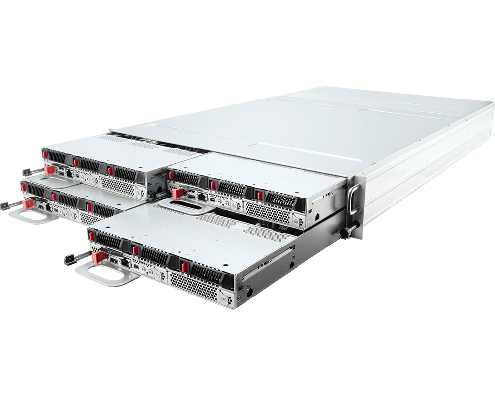
News Posts matching #next generation

Return to Keyword Browsing

NVIDIA cuLitho Computational Lithography Platform is Moving to Production at TSMC

TSMC, the world leader in semiconductor manufacturing, is moving to production with NVIDIA's computational lithography platform, called cuLitho, to accelerate manufacturing and push the limits of physics for the next generation of advanced semiconductor chips. A critical step in the manufacture of computer chips, computational lithography is involved in the transfer of circuitry onto silicon. It requires complex computation - involving electromagnetic physics, photochemistry, computational geometry, iterative optimization and distributed computing. A typical foundry dedicates massive data centers for this computation, and yet this step has traditionally been a bottleneck in bringing new technology nodes and computer architectures to market.

Computational lithography is also the most compute-intensive workload in the entire semiconductor design and manufacturing process. It consumes tens of billions of hours per year on CPUs in the leading-edge foundries. A typical mask set for a chip can take 30 million or more hours of CPU compute time, necessitating large data centers within semiconductor foundries. With accelerated computing, 350 NVIDIA H100 Tensor Core GPU-based systems can now replace 40,000 CPU systems, accelerating production time, while reducing costs, space and power.

LG gram Ready to Define the Next-Gen AI Laptop With New Intel Core Ultra Processors

LG Electronics (LG) is excited to announce that its newest LG gram laptop featuring the Intel Core Ultra processor (Series 2) will be showcased at the Intel Core Ultra Global Launch Event from September 3-8. Renowned for its powerful performance and ultra-lightweight design, the LG gram series now integrates advanced AI capabilities powered by the latest Intel Core Ultra processor. The LG gram 16 Pro, the first model to feature these new Intel processors, will be unveiled before its release at the end of 2024.

As the first on-device AI laptop from the LG gram series, it offers up to an impressive 48 neural processing unit (NPU) tera operations per second (TOPS), setting a new standard for AI PCs and providing the exceptional performance required for Copilot experiences. Powered by the latest Intel Core Ultra processor, the LG gram 16 Pro is now more efficient thanks to advanced AI functionalities such as productivity assistants, text and image creation and collaboration tools. What's more, its extended battery life helps users handle tasks without worry.

Intel "Arrow Lake" and "Lunar Lake" Are Safe from Voltage Stability Issues, Company Reports

Intel's 13th and 14th generation processors, codenamed "Raptor Lake" and "Raptor Lake Refresh," have been notoriously riddled with stability issues over the past few months, up until Intel shipped the 0x129 microcode update on August 10 to fix these issues. However, the upcoming Intel Core Ultra 200 "Arrow Lake" and 200V series "Lunar Lake" processors will not have these issues as the company confirmed that an all-new design is used, even for the segment of power regulation. The official company note states: "Intel confirms that its next generation of processors, codenamed Arrow Lake and Lunar Lake, are not affected by the Vmin Shift Instability issue due to the new architectures powering both product families. Intel will ensure future product families are protected against the Vmin Shift Instability issue as well."

Originally, Intel's analysis for 13th—and 14th-generation processors indicated that stability issues stemmed from excessive voltage during processor operation. These voltage increases led to degradation, raising the minimum voltage necessary for stable performance, which Intel refers to as "Vmin shift." Given that the design phase of new architectures lasts for years, Intel has surely anticipated that the old power delivery could yield problems, and the upcoming CPU generations are now exempt from these issues, bringing stability once again to Intel's platforms. When these new products launch, all eyes will be on the platform's performance, but with a massive interest in stability testing from enthusiasts.

EK Announces Next-Generation Flat Style EK Quantum Combo Units

EK, the leading premium liquid cooling gear manufacturer, is releasing the next generation of its versatile flat-style combo units. EK-Quantum Kinetic³ FLT D5 series pump-reservoir units are equipped with genuine D5 pumps made in Europe, capable of delivering flow rates of 1000 liters per hour with a maximum head pressure of up to 5.2 meters! These new FLT series combo units are available in six different sizes 92 mm, 120 mm, 240 mm, 140 mm, 280 mm, and 360 mm.

The main upgrades of the Kinetic³ combo units include:
  • Additional G1/4" connection ports
  • Front-mounted pump for added versatility
  • Side and back mounting holes for flexibility during installation
  • A custom-made inner O-ring that prevents coolant from seeping between the channels and improves flow
  • Dense LED strip implementation
  • User-friendly LED cover for LED strip service

Intel 18A Powers On, Panther Lake and Clearwater Forest Out of the Fab and Booting OS

Intel today announced that its lead products on Intel 18A, Panther Lake (AI PC client processor) and Clearwater Forest (server processor), are out of the fab and have powered-on and booted operating systems. These milestones were achieved less than two quarters after tape-out, with both products on track to start production in 2025. The company also announced that the first external customer is expected to tape out on Intel 18A in the first half of next year.

"We are pioneering multiple systems foundry technologies for the AI era and delivering a full stack of innovation that's essential to the next generation of products for Intel and our foundry customers. We are encouraged by our progress and are working closely with customers to bring Intel 18A to market in 2025." -Kevin O'Buckley, Intel senior vice president and general manager of Foundry Services

NEO Semiconductor Announces 3D X-AI Chip as HBM Successor

NEO Semiconductor, a leading developer of innovative technologies for 3D NAND flash memory and 3D DRAM, announced today the development of its 3D X-AI chip technology, targeted to replace the current DRAM chips inside high bandwidth memory (HBM) to solve data bus bottlenecks by enabling AI processing in 3D DRAM. 3D X-AI can reduce the huge amount of data transferred between HBM and GPUs during AI workloads. NEO's innovation is set to revolutionize the performance, power consumption, and cost of AI Chips for AI applications like generative AI.

AI Chips with NEO's 3D X-AI technology can achieve:
  • 100X Performance Acceleration: contains 8,000 neuron circuits to perform AI processing in 3D memory.
  • 99% Power Reduction: minimizes the requirement of transferring data to the GPU for calculation, reducing power consumption and heat generation by the data bus.
  • 8X Memory Density: contains 300 memory layers, allowing HBM to store larger AI models.

Marvell Introduces Breakthrough Structera CXL Product Line to Address Server Memory Bandwidth and Capacity Challenges in Cloud Data Centers

Marvell Technology, Inc., a leader in data infrastructure semiconductor solutions, today launched the Marvell Structera product line of Compute Express Link (CXL) devices that enable cloud data center operators to overcome memory performance and scaling challenges in general-purpose servers.

To address memory-intensive applications, data center operators add extra servers to get higher memory bandwidth and higher memory capacity. The compute capabilities from the added processors are typically not utilized for these applications, making the servers inefficient from cost and power perspectives. The CXL industry standard addresses this challenge by enabling new architectures that can efficiently add memory to general-purpose servers.

Ex-Xeon Chief Lisa Spelman Leaves Intel and Joins Cornelis Networks as CEO

Cornelis Networks, a leading independent provider of intelligent, high-performance networking solutions, today announced the appointment of Lisa Spelman as its new chief executive officer (CEO), effective August 15. Spelman joins Cornelis from Intel Corporation, where she held executive leadership roles for more than two decades, including leading the company's core data center business. Spelman will succeed Philip Murphy, who will assume the role of president and chief operating officer (COO).

"Cornelis is unique in having the products, roadmap, and talent to help customers address this issue. I look forward to joining the team to bring their innovations to even more organizations around the globe."

Tenstorrent Launches Next Generation Wormhole-based Developer Kits and Workstations

Tenstorrent is launching their next generation Wormhole chip featuring PCIe cards and workstations designed for developers who are interested in scalability for multi-chip development using Tenstorrent's powerful open-source software stacks.

These Wormhole-based cards and systems are now available for immediate order on tenstorrent.com:
  • Wormhole n150, powered by a single processor
  • Wormhole n300, powered by two processors
  • TT-LoudBox, a developer workstation powered by four Wormhole n300s (eight processors)

Intel Core Ultra 300 Series "Panther Lake" Leaks: 16 CPU Cores, 12 Xe3 GPU Cores, and Five-Tile Package

Intel is preparing to launch its next generation of mobile CPUs with Core Ultra 200 series "Lunar Lake" leading the charge. However, as these processors are about to hit the market, leakers reveal Intel's plans for the next-generation Core Ultra 300 series "Panther Lake". According to rumors, Panther Lake will double the core count of Lunar Lake, which capped out at eight cores. There are several configurations of Panther Lake in the making based on the different combinations of performance (P) "Cougar Cove," efficiency (E) "Skymont," and low power (LP) cores. First is the PTL-U with 4P+0E+4LP cores with four Xe3 "Celestial" GPU cores. This configuration is delivered within a 15 W envelope. Next, we have the PTL-H variant with 4P+8E+4LP cores for a total of 16 cores, with four Xe3 GPU cores, inside a 25 W package. Last but not least, Intel will also make PTL-P SKUs with 4P+8E+4LP cores, with 12 Xe3 cores, to create a potentially decent gaming chip with 25 W of power.

Intel's Panther Lake CPU architecture uses an innovative design approach, utilizing a multi-tile configuration. The processor incorporates five distinct tiles, with three playing active roles in its functionality. The central compute operations are handled by one "Die 4" tile with CPU and NPU, while "Die 1" is dedicated to platform control (PCD). Graphics processing is managed by "Die 5", leveraging Intel's Xe3 technology. Interestingly, two of the five tiles serve a primarily structural purpose. These passive elements are strategically placed to achieve a balanced, rectangular form factor for the chip. This design philosophy echoes a similar strategy employed in Intel's Lunar Lake processors. Panther Lake is poised to offer greater versatility compared to its Lunar Lake counterpart. It's expected to cater to a wider range of market segments and use cases. One notable advancement is the potential for increased memory capacity compared to Lunar Lake, which capped out at 32 GB of LPDDR5X memory running at 8533 MT/s. We can expect to hear more potentially at Intel's upcoming Innovation event in September, while general availability of Panther Lake is expected in late 2025 or early 2026.

HYTE Launches the Next Generation of Y70 Touch Case - Y70 Touch Infinite

HYTE, a leading manufacturer of cutting-edge PC components and peripherals, today announced the next generation of its viral Y70 Touch case, Y70 Touch Infinite, alongside the Y70 Touch Infinite Display Upgrade, as promised to its users. After the unfortunate discontinuation of Y70 Touch in February 2024, HYTE was diligent in its development and pursuit of an infinite touchscreen solution for one of its leading cases.

Y70 Touch Infinite
Introducing Y70 Touch Infinite with a larger 14.5" integrated touchscreen, 688 x 2560 resolution, and 183 PPI for improved compatibility and resource usage. Y70 Touch Infinite boasts a 33% closer dot pitch for a sharper-looking image alongside a 17% brighter LCD panel and a 25% higher contrast ratio. The 60Hz refresh rate with 50% faster pixel response time enables a smoother and more fluid visual experience than its predecessor.
HYTE Y70 Display Upgrade HYTE Milky Y70

AMD Promises Next-Generation Product Announcements in its Computex Keynote

AMD on Monday said that its 2024 Computex Keynote address slated for June 3, will see a slew of next-generation product announcements. "Join us as Dr. Lisa Su delivers the Computex 2024 opening keynote and shares the latest on how AMD and our partners are pushing the envelope with our next generation of high-performance PC, data center and AI solutions," the brief release said.

AMD is widely expected to unveil its next-generation Ryzen 9000 "Strix Point" mobile processors for AI PCs capable of powering the recently announced Microsoft Copilot+, its next-generation Ryzen 9000 "Granite Ridge" desktop processors, its 5th Generation EPYC "Turin" server processors, and possibly even its next-generation Radeon RX RDNA 4 generation. At the heart of all its processor announcements is the new "Zen 5" CPU microarchitecture that's expected to introduce an over 10% IPC improvement with significant improvements in AVX512 performance over "Zen 4," which should benefit certain kinds of AI workloads.

AMD to Redesign Ray Tracing Hardware on RDNA 4

AMD's next generation RDNA 4 graphics architecture is expected to feature a completely new ray tracing engine, Kepler L2, a reliable source with GPU leaks, claims. Currently, AMD uses a component called Ray Accelerator, which performs the most compute-intensive portion of the ray intersection and testing pipeline, while AMD's approach to ray tracing on a hardware level still relies greatly on the shader engines. The company had debuted the ray accelerator with RDNA 2, its first architecture to meet DirectX 12 Ultimate specs, and improved the component with RDNA 3, by optimizing certain aspects of its ray testing, to bring about a 50% improvement in ray intersection performance over RDNA 2.

The way Kepler L2 puts it, RDNA 4 will feature a fundamentally transformed ray tracing hardware solution from the ones on RDNA 2 and RDNA 3. This could probably delegate more of the ray tracing workflow onto fixed-function hardware, unburdening the shader engines further. AMD is expected to debut RDNA 4 with its next line of discrete Radeon RX GPUs in the second half of 2024. Given the chatter about a power-packed event by AMD at Computex, with the company expected to unveil "Zen 5" CPU microarchitecture on both server and client processors; we might expect some talk on RDNA 4, too.

TSMC Celebrates 30th North America Technology Symposium with Innovations Powering AI with Silicon Leadership

TSMC today unveiled its newest semiconductor process, advanced packaging, and 3D IC technologies for powering the next generation of AI innovations with silicon leadership at the Company's 2024 North America Technology Symposium. TSMC debuted the TSMC A16 technology, featuring leading nanosheet transistors with innovative backside power rail solution for production in 2026, bringing greatly improved logic density and performance. TSMC also introduced its System-on-Wafer (TSMC-SoW) technology, an innovative solution to bring revolutionary performance to the wafer level in addressing the future AI requirements for hyperscaler datacenters.

This year marks the 30th anniversary of TSMC's North America Technology Symposium, and more than 2,000 attended the event, growing from less than 100 attendees 30 years ago. The North America Technology Symposium in Santa Clara, California kicks off TSMC Technology Symposiums around the world in the coming months. The symposium also features an "Innovation Zone," designed to highlight the technology achievements of our emerging start-up customers.

Meta Announces New MTIA AI Accelerator with Improved Performance to Ease NVIDIA's Grip

Meta has announced the next generation of its Meta Training and Inference Accelerator (MTIA) chip, which is designed to train and infer AI models at scale. The newest MTIA chip is a second-generation design of Meta's custom silicon for AI, and it is being built on TSMC's 5 nm technology. Running at the frequency of 1.35 GHz, the new chip is getting a boost to 90 Watts of TDP per package compared to just 25 Watts for the first-generation design. Basic Linear Algebra Subprograms (BLAS) processing is where the chip shines, and it includes matrix multiplication and vector/SIMD processing. At GEMM matrix processing, each chip can process 708 TeraFLOPS at INT8 (presumably meant FP8 in the spec) with sparsity, 354 TeraFLOPS without, 354 TeraFLOPS at FP16/BF16 with sparsity, and 177 TeraFLOPS without.

Classical vector and processing is a bit slower at 11.06 TeraFLOPS at INT8 (FP8), 5.53 TeraFLOPS at FP16/BF16, and 2.76 TFLOPS single-precision FP32. The MTIA chip is specifically designed to run AI training and inference on Meta's PyTorch AI framework, with an open-source Triton backend that produces compiler code for optimal performance. Meta uses this for all its Llama models, and with Llama3 just around the corner, it could be trained on these chips. To package it into a system, Meta puts two of these chips onto a board and pairs them with 128 GB of LPDDR5 memory. The board is connected via PCIe Gen 5 to a system where 12 boards are stacked densely. This process is repeated six times in a single rack for 72 boards and 144 chips in a single rack for a total of 101.95 PetaFLOPS, assuming linear scaling at INT8 (FP8) precision. Of course, linear scaling is not quite possible in scale-out systems, which could bring it down to under 100 PetaFLOPS per rack.
Below, you can see images of the chip floorplan, specifications compared to the prior version, as well as the system.

MediaTek Licenses NVIDIA GPU IP for AI-Enhanced Vehicle Processors

NVIDIA has been offering its GPU IP for more than a decade now ever since the introduction of Kepler uArch, and its IP has had relatively low traction in other SoCs. However, that trend seems to be reaching an inflection point as NVIDIA has given MediaTek a license to use its GPU IP to produce the next generation of processors for the auto industry. The newest MediaTek Dimensity Auto Cockpit family consists of CX-1, CY-1, CM-1, and CV-1, where the CX-1 targets premium vehicles, CM targets medium range, and CV targets lower-end vehicles, probably divided by their compute capabilities. The Dimensity Auto Cockpit family is brimming with the latest technology, as the processor core of choice is an Armv9-based design paired with "next-generation" NVIDIA GPU IP, possibly referring to Blackwell, capable of doing ray tracing and DLSS 3, powered by RTX and DLA.

The SoC is supposed to integrate a lot of technology to lower BOM costs of auto manufacturing, and it includes silicon for controlling displays, cameras (advanced HDR ISP), audio streams (multiple audio DSPs), and connectivity (WiFi networking). Interestingly, the SKUs can play movies with AI-enhanced video and support AAA gaming. MediaTek touts the Dimensity Auto Cockpit family with fully local AI processing capabilities, without requiring assistance from outside servers via WiFi, and 3D spatial sensing with driver and occupant monitoring, gaze-aware UI, and natural controls. All of that fits into an SoC fabricated at TSMC's fab on a 3 nm process and runs on the industry-established NVIDIA DRIVE OS.

Silicon Box Announces $3.6 Billion Foundry Deal - New Facility Marked for Northern Italy

Silicon Box, a cutting-edge, advanced panel-level packaging foundry announced its intention to collaborate with the Italian government to invest up to $3.6 billion (€3.2 billion) in Northern Italy, as the site of a new, state-of-the-art semiconductor assembly and test facility. This facility will help meet critical demand for advanced packaging capacity to enable next generation technologies that Silicon Box anticipates by 2028. The multi-year investment will replicate Silicon Box's flagship foundry in Singapore which has proven capability and capacity for the world's most advanced semiconductor packaging solutions, then expand further into 3D integration and testing. When completed, the new facility will support approximately 1,600 Silicon Box employees in Italy. The construction of the facility is also expected to create several thousand more jobs, including eventual hiring by suppliers. Design and planning for the facility will begin immediately, with construction to commence pending European Commission approval of planned financial support by the Italian State.

As well as bringing the most advanced chiplet integration, packaging, and testing to Italy, Silicon Box's manufacturing process is based on panel-level-production; a world leading, first-of-its-kind combination that is already shipping product to customers from its Singapore foundry. Through the investment, Silicon Box has plans for greater innovation and expansion in Europe, and globally. The new integrated production facility is expected to serve as a catalyst for broader ecosystem investments and innovation in Italy, as well as the rest of the European Union.

Microsoft DirectSR Super Resolution API Brings Together DLSS, FSR and XeSS

Microsoft has just announced that their new DirectSR Super Resolution API for DirectX will provide a unified interface for developers to implement super resolution in their games. This means that game studios no longer have to choose between DLSS, FSR, XeSS, or spend additional resources to implement, bug-test and support multiple upscalers. For gamers this is huge news, too, because they will be able to run upscaling in all DirectSR games—no matter the hardware they own. While AMD FSR and Intel XeSS run on all GPUs from all vendors, NVIDIA DLSS is exclusive to Team Green's hardware. With their post, Microsoft also confirms that DirectSR will not replace FSR/DLSS/XeSS with a new upscaler by Microsoft, rather that it builds on existing technologies that are already available, unifying access to them.

While we have to wait until March 21 for more details to be revealed at GDC 2024, Microsoft's Joshua Tucker stated in a blog post: "We're thrilled to announce DirectSR, our new API designed in partnership with GPU hardware vendors to enable seamless integration of Super Resolution (SR) into the next generation of games. Super Resolution is a cutting-edge technique that increases the resolution and visual quality in games. DirectSR is the missing link developers have been waiting for when approaching SR integration, providing a smoother, more efficient experience that scales across hardware. This API enables multi-vendor SR through a common set of inputs and outputs, allowing a single code path to activate a variety of solutions including NVIDIA DLSS Super Resolution, AMD FidelityFX Super Resolution, and Intel XeSS. DirectSR will be available soon in the Agility SDK as a public preview, which will enable developers to test it out and provide feedback. Don't miss our DirectX State of the Union at GDC to catch a sneak peek at how DirectSR can be used with your games!"

Samsung Reportedly Working on Backside Power Supply Tech with 2 Nanometer Process

Samsung and ARM announced a collaborative project last week—the partners are aiming to deliver an "optimized next generation Arm Cortex -X CPU" developed on the latest Gate-All-Around (GAA) process technology. Semiconductor industry watchdogs believe that Samsung Foundry's 3 nm GAA process did not meet sales expectations—reports suggest that many clients decided to pursue advanced three nanometer service options chez TSMC. The South Korean multinational manufacturing conglomerate is setting its sights forward—with an in-progress SF2 GAAFET process in the pipeline—industry insiders reckon that Samsung leadership is hoping to score a major victory within this next-gen market segment.

Lately, important industry figures have been hyping up Backside Power Supply Delivery Network (BSPDN) technology—recent Intel Foundry Services (IFS) press material lays claim to several technological innovations. A prime example being an ambitious five-nodes-in-four-years (5N4Y) process roadmap that: "remains on track and will deliver the industry's first backside power solution." A Chosun Business report proposes that Samsung is working on Backside Power Supply designs—a possible "game changer" when combined with in-house 2 nm SF2 GAAFET. Early experiments, allegedly, involving two unidentified ARM cores have exceeded expectations—according to Chosun's sources, engineers were able to: "reduce the chip area by 10% and 19%, respectively, and succeeded in improving chip performance and frequency efficiency to a single-digit level." Samsung Foundry could be adjusting its mass production timetables, based on freshly reported technological breakthroughs—SF2 GAAFET + BSPDN designs could arrive before the original targeted year of 2027. Prior to the latest developments, Samsung's BSPDN tech was linked to a futuristic 1.7 nm line.

Qualcomm AI Hub Introduced at MWC 2024

Qualcomm Technologies, Inc. unveiled its latest advancements in artificial intelligence (AI) at Mobile World Congress (MWC) Barcelona. From the new Qualcomm AI Hub, to cutting-edge research breakthroughs and a display of commercial AI-enabled devices, Qualcomm Technologies is empowering developers and revolutionizing user experiences across a wide range of devices powered by Snapdragon and Qualcomm platforms.

"With Snapdragon 8 Gen 3 for smartphones and Snapdragon X Elite for PCs, we sparked commercialization of on-device AI at scale. Now with the Qualcomm AI Hub, we will empower developers to fully harness the potential of these cutting-edge technologies and create captivating AI-enabled apps," said Durga Malladi, senior vice president and general manager, technology planning and edge solutions, Qualcomm Technologies, Inc. "The Qualcomm AI Hub provides developers with a comprehensive AI model library to quickly and easily integrate pre-optimized AI models into their applications, leading to faster, more reliable and private user experiences."

Fibocom Intros MediaTek-powered 5G RedCap Module FM330

Fibocom, a global leading provider of IoT (Internet of Things) wireless solutions and wireless communication modules, launches a new series of 5G RedCap module integrated with MediaTek's T300 5G modem, which is the world's first 6 nm radio frequency system-on-chip (RFSOC) single die solution for 5G RedCap. By integrating a single-core Arm Cortex-A3 processor in a significantly compact PCB area, the FM330 series are optimal solutions that offer extended coverage, increased network efficiency and device battery life for industry customers.

Compliant with 3GPP R17 standards, the FM330 series supports mainstream 5G frequency bands worldwide and is capable of reaching a maximum bandwidth of 20 MHz, thus ensuring the peak data rate of up to 227 Mbps downlink and 122 Mbps uplink, sufficient to meet the demand for 5G applications with less data throughput while balancing the power efficiency. In hardware design, it adopts the M.2form factor measured at 30x42mm benefiting from the unique RFSOC solution integrated with T300, in addition to the optimized antenna design in 1T2R, which significantly saves the PCB area. Moreover, FM330 series is pin-compatible with Fibocom LTE Cat 6 module FM101, easing the concerns for customers' migration from 4G to 5G. Furthermore, the module provides 64QAM/256QAM (optional) modulation scheme to greatly optimize the cost and size.

Intel CEO Discloses TSMC Production Details: N3 for Arrow Lake & N3B for Lunar Lake

Intel CEO Pat Gelsinger engaged with press/media representatives following the conclusion of his IFS Direct Connect 2024 keynote speech—when asked about Team Blue's ongoing relationship with TSMC, he confirmed that their manufacturing agreement has advanced from "5 nm to 3 nm." According to a China Times news article: "Gelsinger also confirmed the expansion of orders to TSMC, confirming that TSMC will hold orders for Intel's Arrow and Lunar Lake CPU, GPU, and NPU chips this year, and will produce them using the N3B process, officially ushering in the Intel notebook platform that the outside world has been waiting for many years." Past leaks have indicated that Intel's Arrow Lake processor family will have CPU tiles based on their in-house 20A process, while TSMC takes care of the GPU tile aspect with their 3 nm N3 process node.

That generation is expected to launch later this year—the now "officially confirmed" upgrade to 3 nm should produce pleasing performance and efficiency improvements. The current crop of Core Ultra "Meteor Lake" mobile processors has struggled with the latter, especially when compared to rivals. Lunar Lake is marked down for a 2025 launch window, so some aspects of its internal workings remain a mystery—Gelsinger has confirmed that TSMC's N3B is in the picture, but no official source has disclosed their in-house manufacturing choice(s) for LNL chips. Wccftech believes that Lunar Lake will: "utilize the same P-Core (Lion Cove) and brand-new E-Core (Skymont) core architecture which are expected to be fabricated on the 20A node. But that might also be limited to the CPU tile. The GPU tile will be a significant upgrade over the Meteor Lake and Arrow Lake CPUs since Lunar Lake ditches Alchemist and goes for the next-gen graphics architecture codenamed "Battlemage" (AKA Xe2-LPG)." Late January whispers pointed to Intel and TSMC partnering up on a 2 nanometer process for the "Nova Lake" processor generation—perhaps a very distant prospect (2026).

Arm Launches Next-Generation Neoverse CSS V3 and N3 Designs for Cloud, HPC, and AI Acceleration

Last year, Arm introduced its Neoverse Compute Subsystem (CSS) for the N2 and V2 series of data center processors, providing a reference platform for the development of efficient Arm-based chips. Major cloud service providers like AWS with Graviton 4 and Trainuium 2, Microsoft with Cobalt 100 and Maia 100, and even NVIDIA with Grace CPU and Bluefield DPUs are already utilizing custom Arm server CPU and accelerator designs based on the CSS foundation in their data centers. The CSS allows hyperscalers to optimize Arm processor designs specifically for their workloads, focusing on efficiency rather than outright performance. Today, Arm has unveiled the next generation CSS N3 and V3 for even greater efficiency and AI inferencing capabilities. The N3 design provides up to 32 high-efficiency cores per die with improved branch prediction and larger caches to boost AI performance by 196%, while the V3 design scales up to 64 cores and is 50% faster overall than previous generations.

Both the N3 and V3 leverage advanced features like DDR5, PCIe 5.0, CXL 3.0, and chiplet architecture, continuing Arm's push to make chiplets the standard for data center and cloud architectures. The chiplet approach enables customers to connect their own accelerators and other chiplets to the Arm cores via UCIe interfaces, reducing costs and time-to-market. Looking ahead, Arm has a clear roadmap for its Neoverse platform. The upcoming CSS V4 "Adonis" and N4 "Dionysus" designs will build on the improvements in the N3 and V3, advancing Arm's goal of greater efficiency and performance using optimized chiplet architectures. As more major data center operators introduce custom Arm-based designs, the Neoverse CSS aims to provide a flexible, efficient foundation to power the next generation of cloud computing.

SoftBank Founder Wants $100 Billion to Compete with NVIDIA's AI

Japanese tech billionaire and founder of the SoftBank Group, Masayoshi Son, is embarking on a hugely ambitious new project to build an AI chip company that aims to rival NVIDIA, the current leader in AI semiconductor solutions. Codenamed "Izanagi" after the Japanese god of creation, Son aims to raise up to $100 billion in funding for the new venture. With his company SoftBank having recently scaled back investments in startups, Son is now setting his sights on the red-hot AI chip sector. Izanagi would leverage SoftBank's existing chip design firm, Arm, to develop advanced semiconductors tailored for artificial intelligence computing. The startup would use Arm's instruction set for the chip's processing elements. This could pit Izanagi directly against NVIDIA's leadership position in AI chips. Son has a chest of $41 billion in cash at SoftBank that he can deploy for Izanagi.

Additionally, he is courting sovereign wealth funds in the Middle East to contribute up to $70 billion in additional capital. In total, Son may be seeking up to $100 billion to bankroll Izanagi into a chip powerhouse. AI chips are seeing surging demand as machine learning and neural networks require specialized semiconductors that can process massive datasets. NVIDIA and other names like Intel, AMD, and select startups have capitalized on this trend. However, Son believes the market has room for another major player. Izanagi would focus squarely on developing bleeding-edge AI chip architectures to power the next generation of artificial intelligence applications. It is still unclear if this would be an AI training or AI inference project, but given that the training market is currently bigger as we are in the early buildout phase of AI infrastructure, the consensus might settle on training. With his track record of bold bets, Son is aiming very high with Izanagi. It's a hugely ambitious goal, but Son has defied expectations before. Project Izanagi will test the limits of even his vision and financial firepower.

Lenovo Reportedly Showcasing Prototype Transparent OLED Notebook at MWC 2024

Attention is now turning to the late February Mobile World Congress (WWC) 2024 trade show—following journos recovering from their recent CES gauntlet-esque ordeals. An exclusive Windows Report piece proposes that Lenovo representatives will be heading to Barcelona with a very special next generation laptop in hand. The publication has a outed a number of upcoming portable devices, two weeks prior to Lenovo's intended showcase (February 26 - 29)—we witnessed a similar occurrence last year with WinFuture leaking Microsoft's September Surface refreshes. Six notebook refreshes (ThinkPad and ThinkBook) are mentioned in the latest report, as well as Gen 2 version of Lenovo's ThinkVision M14T portable monitor.

The alleged headliner seems to be a concept model, that slides into the company's ThinkBook range—Windows Report has leaked heavily watermarked images, but little in the way of technical specifications: "Lenovo's transparent laptop features a bezel-less design, with the display being completely see-through. The deck also seems completely transparent, with the main components being housed in and under the chin, which is the area that's not transparent. There's also a non-transparent slim frame that surrounds the entire deck, probably housing the ports." An anonymous source reckons that the transparent OLED ThinkBook runs on Windows 11, and Lenovo's tried and trusted design language is very apparent (when in use).
Return to Keyword Browsing
Oct 18th, 2024 02:19 EDT change timezone

New Forum Posts

Popular Reviews

Controversial News Posts