Wednesday, August 19th 2009

Clarkdale IGP Detailed, Tested
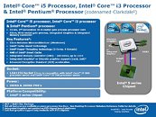
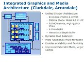
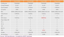
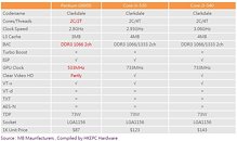
Intel's upcoming "Clarkdale" is special for two reasons: it is the first 32 nm based processor from Intel, and that it's the first processor that comes with a graphics processor built in, something AMD conceptualized a long time ago. Under the hood (read: integrated heat-spreader), Clarkdale is a busy package, that holds a CPU complex die (that houses the main processing cores, cache, a dual-channel DDR3 integrated memory controller, and a Quickpath interconnect controller, that connects the die to its neighbor, a northbridge-iGraphics die that houses most northbridge components including a PCI-Express 2.0 root complex, the star-attraction IGP and a DMI connection to the "platform controller hub (PCH)".As the industry is gearing up for a gala launch of the socket LGA-1156 platform, almost every processor and motherboard making news leaves out the iGraphics component of these processors, simply because the first LGA-1156 processors to hit the scene, the quad-core "Lynnfield" lacks an IGP, and that it's much talked about sidekick the P55 chipset lacks the necessary component that lets the platform make use of the IGP. Dubbed Intel Flexible Display Interface (FDI), a component links the IGP to its display connectors on the board. Other members in Intel's upcoming 5-series chipsets, namely H55, H57, and Q55 as detailed earlier, feature FDI.The IGP itself uses a fairly conventional design, and focuses on essentially light 3D, and HD video acceleration, as today's consumer OSes are using user interfaces that heavily make use of hardware 3D acceleration, and more applications are using light 3D. With this being the generation that's moving towards HD video, it's a good idea to have at least an IGP that has what it takes to support all industry HD video standards for smooth playback. The IGP is DirectX 10 Shader Model 4.0 compliant, for starters, so it might technically be eligible to accelerate compute shader applications.Back when the processor model number scheme of Intel's Clarkdale-based dual-core processors first surfaced, the presence of a "Core i5 661" with the same specifications as the "Core i5 660" baffled us. The missing piece of the puzzle turned out to be its IGP, which has a higher core speed of 900 MHz. Other Core i5 and Core i3 "Clarkdale" processors have their IGPs running at 733 MHz instead. As a result of this seemingly small speed-bump, the overall processor TDP shoots up from 73W to 89W. Pentium G6950 has a much lower IGP core speed of 533 MHz, though it doesn't affect the TDP one bit. So there's more to it than IGP speeds.Finally, it boils down to performance. The Clarkdale IGP was pitted against Intel GMA X4500HD that's found on current Intel G45 chipset, and NVIDIA GeForce 9400 found on some high-end MCP7A-based motherboards, including the ION platform. While the superior graphics processing capabilities of the GeForce 9400 makes it almost inconsequential, the Clarkdale IGP performs almost twice as fast as GMA X4500HD overall. With HD video playback tests, the objective is to measure CPU usage. Lower the usage, the better. While the GeForce 9400 took the lead in most tests, again, the Clarkdale IGP outperformed its predecessor. It aced the Dual Stream H.264 20Mbps test with the lowest CPU usage.With P55 and Lynnfield hogging most of the limelight, not much more is known about the IGP+H5x platform. Hopefully, we get to know more in Q1 2010, when Intel plans its second big wave of CPU launches.
Source:
HKEPC



28 Comments on Clarkdale IGP Detailed, Tested
But im not getting it.(as solely a gamer):)
Off topic but check that dude's eyebrows in the first pic there huuuuge.
aside from that more stuff coming out, im not sure i can see these selling lots in the first year, I mean most peoples c2, c2q, PHenII and i7's are more than enough, but who knows.
The 661's TDP jumped by so much not because it uses that much, but because 87W is the next "standard" TDP Intel wants for this generation.
Im not seeing which chip (533Mhz/733Mhz/900Mhz) was benchmarked.
And I think it's cool that they can cram all these things on a single chip, but I'm not sure about the point of it. Cutting production costs and all that, but still..
I like how the chart says 87W, the text says 89W, and the reasonable number is 82W (same as the LP quads).
Think Apple I, II, 8-bit computing, all graphics were done directly by the CPU. There was a linear memory map that the CPU shared between "programs, "OS", "data" and "graphics". It was the Amiga that was the first computer to do hardware acceleration outside of the CPU.
For PCs, it was mostly Windows that drove the implementation of hardware graphics... due to the massive amounts of data that needed to be moved around to create and drag windows etc. MS developed Windows API and the rest is 2D history.
The next gen. of GPUs were driven by 3D games. :-)
The point about sticking separate purpose dies into one package is however true. But I wonder what came first: the idea of sticking 2 identical dies together (as in dual core computing) or the idea of sticking 2 asymetric dies together (as in one CPU and one GPU).
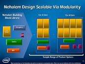
Oophs! Someone made a graphical typo... shouldnt there be an example on the RHS including the GPU when talking about Clarkdale? LOL. Brilliant engineers at Intel. Sh17, l4zy or stup1d marketing team.
However, CPUs started developing special instructions for shift large blocks of memory around with just one instruction. There is a blurry line between some CPU instructions and GPU instructions. Only recently with 3D and shaders has that difference become more distinct. Point being: Sticking a GPU onto a CPU die is NOTHING MORE CLEVER OR ORIGINAL than sticking x87 (maths and SSE) onto the same die as the CPU.
Next up; GPU is a CPU (CUDA)
Next up; Larrabee
Next up; CPU less computers (x86 Larrabee based PCs)