Tuesday, March 2nd 2010

GeForce GTX 480 PCB and Cooling Assembly Pictured
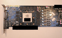
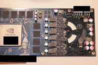
Sources wanting anonymity sent these pictures of PCB and cooling assembly to sections of the media. The PCB is that of the GeForce GTX 480, and is NVIDIA's reference design. It gives away a fair amount of information about the card that has created quite some hype over the months, which is slated for release on March 26. To begin with, the GF100 GPU on which GTX 480 is based, uses essentially the same type of package as the GT200 and G80. To help cool the large die (with a 3 billion-strong transistor count), an integrated heatspreader (IHS) is used. However, unlike with the G80 and GT200 (past two generations of extreme performance GPUs from NVIDIA), the display logic is integrated into the GPU package, instead of being spun off into NVIO processors.
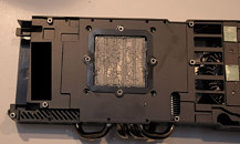
With 12 memory chips on board, the GPU connects to them over a 384-bit wide memory interface. The reference design board is expected to have 1536 MB (1.5 GB) of memory on it. There's also an unusual amount of simplicity to the board design and choice of components. The GPU is powered by a 6-phase vGPU circuit using more standard DPAK MOSFETs. There is a 2-phase vMem circuit. With wide open spaces in the PCB, NVIDIA actually made two cutouts to help the blower's air intake.Power is drawn from an 8-pin and a 6-pin power connector. Fan connects over a standard 4-pin PWM controlled line, while the white 2-pin connector in the picture powers an illuminated GeForce logo on the top of the card (next to the power inputs). Connectivity includes two DVI-D, and a mini HDMI connector. The PCB itself seems to be about as long as reference GeForce GTX 280 boards. The cooling assembly doesn't show off lavish use of copper, but looks equally complex as older cooling assemblies by the company for such GPUs.
Source:
Tweakers.net
With 12 memory chips on board, the GPU connects to them over a 384-bit wide memory interface. The reference design board is expected to have 1536 MB (1.5 GB) of memory on it. There's also an unusual amount of simplicity to the board design and choice of components. The GPU is powered by a 6-phase vGPU circuit using more standard DPAK MOSFETs. There is a 2-phase vMem circuit. With wide open spaces in the PCB, NVIDIA actually made two cutouts to help the blower's air intake.Power is drawn from an 8-pin and a 6-pin power connector. Fan connects over a standard 4-pin PWM controlled line, while the white 2-pin connector in the picture powers an illuminated GeForce logo on the top of the card (next to the power inputs). Connectivity includes two DVI-D, and a mini HDMI connector. The PCB itself seems to be about as long as reference GeForce GTX 280 boards. The cooling assembly doesn't show off lavish use of copper, but looks equally complex as older cooling assemblies by the company for such GPUs.


93 Comments on GeForce GTX 480 PCB and Cooling Assembly Pictured
the copper on outdoor AC units along beaches can still last for years, maybe no more than 10, but when was the last time you used a 10 year old video card.
imo nickel plating is just over doing it, or just plain ol eye candy.
just plain copper (not the soft kind) is all you need imo.
I hope it can beat 5970 with just this one card...
As I'm an user with a silent sys, this is most disturbing. Whatever the speed may be ... and no, you can't get rid of it always when deactivating vsync.
*drool* *sigh* *Oh yeah baby don't stop*:nutkick::toast::slap::respect:
I've seen a fair few in my time as well :laugh:
@ Cleorina, don't you think you should maybe wait for reviews before deciding to buy the card?
Won't be getting one of these myself, settled on 5770 now, will grab another one later if I need more power, for now @1ghz its plenty.
What about the other one?
:D