Tuesday, March 2nd 2010

GeForce GTX 480 PCB and Cooling Assembly Pictured
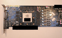
Sources wanting anonymity sent these pictures of PCB and cooling assembly to sections of the media. The PCB is that of the GeForce GTX 480, and is NVIDIA's reference design. It gives away a fair amount of information about the card that has created quite some hype over the months, which is slated for release on March 26. To begin with, the GF100 GPU on which GTX 480 is based, uses essentially the same type of package as the GT200 and G80. To help cool the large die (with a 3 billion-strong transistor count), an integrated heatspreader (IHS) is used. However, unlike with the G80 and GT200 (past two generations of extreme performance GPUs from NVIDIA), the display logic is integrated into the GPU package, instead of being spun off into NVIO processors.
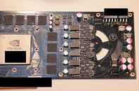
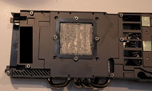
With 12 memory chips on board, the GPU connects to them over a 384-bit wide memory interface. The reference design board is expected to have 1536 MB (1.5 GB) of memory on it. There's also an unusual amount of simplicity to the board design and choice of components. The GPU is powered by a 6-phase vGPU circuit using more standard DPAK MOSFETs. There is a 2-phase vMem circuit. With wide open spaces in the PCB, NVIDIA actually made two cutouts to help the blower's air intake.Power is drawn from an 8-pin and a 6-pin power connector. Fan connects over a standard 4-pin PWM controlled line, while the white 2-pin connector in the picture powers an illuminated GeForce logo on the top of the card (next to the power inputs). Connectivity includes two DVI-D, and a mini HDMI connector. The PCB itself seems to be about as long as reference GeForce GTX 280 boards. The cooling assembly doesn't show off lavish use of copper, but looks equally complex as older cooling assemblies by the company for such GPUs.
Source:
Tweakers.net
With 12 memory chips on board, the GPU connects to them over a 384-bit wide memory interface. The reference design board is expected to have 1536 MB (1.5 GB) of memory on it. There's also an unusual amount of simplicity to the board design and choice of components. The GPU is powered by a 6-phase vGPU circuit using more standard DPAK MOSFETs. There is a 2-phase vMem circuit. With wide open spaces in the PCB, NVIDIA actually made two cutouts to help the blower's air intake.Power is drawn from an 8-pin and a 6-pin power connector. Fan connects over a standard 4-pin PWM controlled line, while the white 2-pin connector in the picture powers an illuminated GeForce logo on the top of the card (next to the power inputs). Connectivity includes two DVI-D, and a mini HDMI connector. The PCB itself seems to be about as long as reference GeForce GTX 280 boards. The cooling assembly doesn't show off lavish use of copper, but looks equally complex as older cooling assemblies by the company for such GPUs.


93 Comments on GeForce GTX 480 PCB and Cooling Assembly Pictured
The boxes are "real" (read below) without a doubt.I don't think that. This is what KainX mentioned in the GTX400 series thread:I agree 100% with this.
It has heatpipes yes, but that base is clearly a just a flat base, they probably just apply the TIM in streaks.
( note there's more tim lines then heatpipes , if those lines were from DHT there would be 5 heatpipes, not 4)
TIM just applied in streaks? :roll:
That is not feasible with an underlying pattern as seen in the photo, and due to the core being flat with applied pressure would flatten it out and rule out that bizzare theory.
it's what it looks like to me, especially considering the lines of tim are raised rather then indented/same level as they would be if it was tim building up between heatpipes.
edit* at your edit, you'd be surprised when it comes to cheap shitty tim .
I've had lines on old matrox video cards ( only 2) and there is not shitting way they had heatpipes let alone DHT XD
If it is DHT, I will eat my words I assure you, how ever its just to perfect in my opinion, if it is DHT its the best implementation I've ever seen.
Still wondering where that 5th heatpipe goes to.
As for the 5th heatpipe, maybe there isn't one. The 5th space might just be a filler, to make the base large enough to cover the entire IHS of the GPU.
*scarpers*
Anyhow, GTX 280 had seven (7) heatpipes, this one has at least those 5. I'll link a picture here from accelero thread in a moment. edit: 4th picture here gives an idea where rest of the pipes go: forums.techpowerup.com/showpost.php?p=1282201&postcount=11
Compare the base to my avatar and just think NVIDIA-amount of TIM on top of it and that is what you get. They like to slap it a lot!
Also the suction force is massive with the IHS and you can't rotate, so you end with some paste 'ripped' upwards.Both AMD and Intel have IHS in their CPU making direct touch more usable. Only NVIDIA has GPU IHS and only GT200 series and Fermi. You have 5 pipes you need 5 pipes area to cool, bare core would only touch about 3.The stock NVIDIA paste isn't that bad, they just use too much of it :D But now it actually works in this case, as the extra paste fills the heatpipe sidewall holes and doesn't need any fancy to the pipes application that would add cost.
Although coolers are 95% of the card, so you may be right.
But of course they would test these things before release so they would compensate somewhere...
^^ that would be sort of what my card design would look like. :cool:
Dont lie... you would buy one. I know im getting 2 :D