Monday, September 27th 2010

AMD Radeon HD 6700 Series ''Barts'' Specs Sheet Surfaces
Here is the slide we've been waiting for, the specs sheet of AMD's next-generation Radeon HD 6700 series GPUs, based on a new, radically redesigned core, codenamed "Barts". The XT variant denotes Radeon HD 6770, and Pro denotes HD 6750. AMD claims that the HD 6700 series will pack "Twice the Horsepower", over previous generation HD 5700 series. Compared to the "Juniper" die that went into making the Radeon HD 5700 series, Barts features twice the memory bandwidth thanks to its 256-bit wide high-speed memory interface, key components such as the SIMD arrays split into two blocks (like on Cypress), and we're now getting to learn that it uses a more efficient 4-D stream processor design. There are 1280 stream processors available to the HD 6770 (Barts XT), and 1120 stream processors to the HD 6750 (Barts Pro). Both SKUs use the full 256-bit memory bus width.
The most interesting specification here is the shader compute power. Barts XT churns out 2.3 TFLOP/s with 1280 stream processors, GPU clocked at 900 MHz, while the Radeon HD 5870 manages 2.72 TFLOP/s with 1600 stream processors, 850 MHz. So indeed the redesigned SIMD core is working its magic. Z/Stencil performance also shot up more than 100% over the Radeon HD 5700 series. Both the HD 6770 and HD 6750 will be equipped with 5 GT/s memory chips, at least on the reference-design cards, which are technically capable of running at 1250 MHz (5 GHz effective), though are clocked at 1050 MHz (4.20 GHz effective) on HD 6770, and 1000 MHz (4 GHz effective) on HD 6750. Although these design changes will inevitably result in a larger die compared to Juniper, it could still be smaller than Cypress, and hence, more energy-efficient.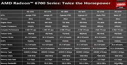
Source:
PCinLife
The most interesting specification here is the shader compute power. Barts XT churns out 2.3 TFLOP/s with 1280 stream processors, GPU clocked at 900 MHz, while the Radeon HD 5870 manages 2.72 TFLOP/s with 1600 stream processors, 850 MHz. So indeed the redesigned SIMD core is working its magic. Z/Stencil performance also shot up more than 100% over the Radeon HD 5700 series. Both the HD 6770 and HD 6750 will be equipped with 5 GT/s memory chips, at least on the reference-design cards, which are technically capable of running at 1250 MHz (5 GHz effective), though are clocked at 1050 MHz (4.20 GHz effective) on HD 6770, and 1000 MHz (4 GHz effective) on HD 6750. Although these design changes will inevitably result in a larger die compared to Juniper, it could still be smaller than Cypress, and hence, more energy-efficient.

245 Comments on AMD Radeon HD 6700 Series ''Barts'' Specs Sheet Surfaces
Using the comparison between the 5830 and the 5770, throws up some odd results, as well as what you have mentioned, despite having double the memory bus it has the same ROP count as the 5770 but were you aware, despite it having double the memory bus, the 5830 is actually SLOWER in pixel fill rate than the 5770, now thats for a couple of reasons but my point is Bus and ROP count are just ingredients in the overall performance, people seem to get too hung up on it, you can get to a point where too many ROP's actually strangle performance and show little improvement where other ingredients can give a greater boost.
Now if we do see a 512bit bus..... and I am not saying we won't, then as you have said, there is more potential there, but with that comes a fairly large hike in prices, I have some doubts that AMD want to go down that route personally, although maybe on just the one top end card.......... my point all along has simply been 2 fold.......
1. Currently I beleive there are limitations on ROP count against Memory Bus size, you aint gonna get 64 ROP's on a 256bit wide bus.
2. There are a lot more factors to overall performance than just bus size and ROP count.
Simple as that really.
I think it is more likely that Cayman will have 384-bit memory, but I also think that it might take less board real estate to simply double the ROPs per memory controller. As for the bandwidth argument, even with GF104 having less bandwidth than Cypress, it seems to have greater ROP performance. Doubling the ROPs may be overkill, but Cayman needs at least double the ROPs performance of Barts to take on GF100 in those applications where ROPs are the limitation.
:eek::eek::eek:
In no way am I giving credibility to the information we have, but just saying that at this point that specs sheet is not one bit more credible.
to be honest as it gets closer to release (whenever it may be) it's time to ignore all the "leaks" and just wait for amd to say something official.
I still think that Barts will have 1024 shaders, with Barts XT shipping with 960 shaders active. I think yields of Barts XT will be too low to justify completely replacing Cypress Pro with Barts without a defect tolerant design. However yield of defect free Barts GPUs would be adequate for fully functional GPUs to be used in a dual GPU product. Along those same lines of logic, there should be too few Barts GPUs with defective ROPs to justify a mass market product like Cypress LE, but if these GPUs could be salvaged for a dual GPU product.
This could also explain the Radeon HD 6990. If Cayman XT is, like GTX 480, a cut down Cayman, and called the Radeon HD 6870, then if the dual GPU variant uses fully functional GPUs, it would make sense to call it a Radeon HD 6990 to signify it is more than a dual Radeon HD 6870.
just a question. what do you need so many shader for if your frame rate won't increase from 200 fps to 800 fps... just being feature rich? folding@home is generally garbage for vast high end gamer and "NO ONE WILL BUY A GFX JUST TO RUN FOLDING@HOME TO SAVE THE MANKIND WHILE CAN'T DO SHIT ON FRAME RATE" if human would die then let them all die....simple.
i would personally throw 500 dollars into water than save human race
anway read below post before you start think 32rop, 256bus with ridiculous 2560 shader will hit to the market with such bad scaling design.hard fact, however people just don't listenof cause you can not boost up performance by just adding rop/bus. you also can't just add ALU without major increase on rops/bus
this is no long speculation, this is fact! we all know shader cost 60% die space in current evergreen design and adding more then twice shader is non sense and make gpu as big as fermi while no frame rate gain and bad scaling is just plenty stupid. you can add more shader on 3870 is because r670 only has die size of 179mm^2 and 282mm^2 in 4870. increase roughly 60% while adding extra 100ALU/24TMU&SIMD cluster.but if we speculate this on cayman it will be 534mm^2 if you design to add more ALU like it did on r770. you fail one thing, if cayman is ONLY 20% gain in performance over barts then why is amd bother to make it out if it's only 20% over a mid range card while having die size of 500mm^2?? a 480:96:64 will have better scaling and frame rate burst over a 1280: (128)64:32.
guess you didn't know anything about how a gpu work. ALU in gpu are act as program decoder and material generator. while rops(Raster Operations Pipeline or Render Output Units in nvidia) are operate as material/texture loading and instruction processed by shader/ALU and finalize. more ALU don't ensure performance boost, in extreme case like highest detail/AA/AF it helps frame rate from dropping in serious margin. for example r670 and r770 don't see much of difference in fps when comes to lower detail/lighting and frame rate are mostly identical except fps. but when come to extreme detail r770 will take advantage because of shader and drop less than r670. however both r670 and r770 having little difference in pixel fill rate except r770 having higher clock and given little more fps. so you want more frame rate then you will need more rops.
and again the 5850 and the 5870 have the came config only different shaders and clocks, what i refered to in my above post is that clocks makes up 99% of the performance difference between the two cards and when you match their clock speeds on the same rig, the 5870 will barely edge out the 5850 at the same clock speeds. Proving that the shader difference between the two doesn't affect performance significantly.
now doubling the shader count might, but not likly enough to grant as much a performance difference as ther eis between the 5870 and 5770 which regarldless will skew pucharse decision away from the highend parts. Being that highend parts already sell less than midrange and are more expensive to manufacturer it could be a costly decision.
don't know why you posted this as it proves my point, since the 5770 has the same rop/tmu/memory bit per shader balance as the the 5870 it has a nice scalable architecture that as you pointed out has a better fillrate than the 5830 depite the fact that the 5830 has 40% more shaders. so...shaders again aren't enough on their own. They need the raw hp of the rop combined with the tmu to get the job done. And no you comclusion based on the data is incorrect, the 5830 has a SHADER bottleneck, not an rop/tmu one. that's why the 5770 with 40% less shaders and 40% less tmu's can have a higher fillrate. (granting the 200MHZ memory and 50MHZ core increase in clock speed on the 5770 might be helping the fillrate).
based on what we know about ati, though they cannot increase the rop count per memory bit in a series,they can disable them second thing we know is that cypress was essentially two seperate cores on a single die and juniper was a single of those cores.
it is possible that ATI/AMD already have a working core with 64 rops on a 256bit bus and we're seeign half of that on barts. another thing to keep in mind is that a few years ago 16 rop's were the max ati could do on a 256-bit bus, so at the time I could have argued that they couldn't put 32 rops on that bus width, I would have been wrong.
besides the fact I don't care if they have to go to a 384-bit bus width with 48 rop's, caymen needs to increase the rop count as well as shaders and tmu's to fit in with barts in the lineup otherwise barts will be the odd man out and steal the sales.
Second, while it is common to quote 1600 for the number of shaders in Cypress, Cypress actually has 1600 ALUs organized as 320 shaders, that are arranged in 20 SIMD pipelines having 16 shaders and 4 TMUs each. Each shader has 4 simple ALUs and 1 complex ALU. Barts/Cayman is supposed to have 4 moderate complexity ALUs per shader.
Barts/Cayman are not derivatives of Juniper or Cypress. They were designed in parallel with Evergreen by the team(s) that designed RV7xx, including RV740. The engineer that was interviewed stated that the 4 ALU per shader design of Northern Islands took up slightly less space per shader than the 4+1 ALU design of Cypress while delivering between 1.5x to 1.8x the performance per shader of Cypress. The engineer might have meant 1.5x to 1.8x the performance per ALU, deliberately using the wrong term to make things clearer to the interviewer that often mentioned the 1600 shaders of Cypress.
The Radeon HD 5830 has the same number of ROPs and memory controllers as the Radeon HD 4870/4890, and falls between the two of them in average performance despite having 1.4x the number of SIMD pipelines. Chances are that it is not the performance of the individual shaders/TMUs that is crippling Cypress, but the SIMD control logic. My guess is that the NI design team went with a 4 moderate complexity ALU design for NI to simplify the control logic, thus enabling them to achieve at least the per shader performance of RV770 while implementing double precision floating point, as well as the DX11 features. Just getting NI to RV770 level per ALU performance would have given NI 12% higher performance per shader than Cypress. And it is possible that other improvements, including higher utilization of the ALUs due to fewer of them per shader and the number of ALUs per shader being a power of two, increased performance per shader to within 95% of the 4+1 ALU shaders. Thus the 1.5x to 1.8x figure quoted.
My guess is that, since the small die size strategy was well established at the time NI was being designed, and 32nm allows for just a bit over 56% more transistors per mm2 versus 40nm, and the 4 ALU shader design is only slightly smaller than the 4+1 ALU shader design, Turks was to be 1.6x Redwood, Barts 1.6x Juniper, and Cayman 1.6x Cypress with regards to shaders/SIMD pipelines. This would make Turks 128 shaders(512 ALUs), Barts 256 shaders (1024 ALUs), and Cayman 512 shaders (2048 ALUs). When 40nm was cancelled, only Cayman had to be cut down, and this was only to keep the TDP within the limits of what was needed to produce a dual GPU "Cayman".
Bus width is primarily a function of die size, and since Barts would have had about the same die size as Juniper at 32nm, Barts would have started with a 128-bit bus. But with Barts having over 50% more core performance than Juniper, there would have been a push towards either increasing the number of ROPs per memory controller by at least 50% or increasing the memory width by 50%. If they went with the memory width solution, Barts would have had a 192-bit wide bus at 32nm. Cayman was probably not large enough for a 384-bit memory bus at 32nm, so my guess is that the number of ROPs per memory controller was increased.
If indeed the Radeon HD 2900 GT had 12 ROPs (persumably 16 total with 4 disabled) it is Cayman might have had 12 ROPs per memory controller at 32nm. Well actually 16 ROPs per memory controller organized as four clusters of 4 ROPs each, with one ROP cluster per memory controller serving as a spare. I estimate that, at the time the GTX 480 was introduced, approximately 14% of all Radeon HD 5850/5870 yield was being lost to defective ROP clusters. At the time the Radeon HD 5830 was introduced this yield loss to defective ROP clusters would have been higher, thus the need to salvage a part with one ROP cluster per memory controller disabled. ATI probably anticipated similar yield problems at 32nm, and at least wanted one spare ROP cluster per memory controller available to improve yields, so the design could have been three ROP clusters per memory contoller with the third serving only as a spare, but more likely, with the need for 50% higher ROP performance to match the 50% higher core performance, ROP clusters per memory controller were doubled, with the fourth ROP cluster per memory controller serving as a spare.
With 32nm being cancelled and NI reimplemented at 40nm, die size grew, and there was increased perimeter on which to implement edge pads, enabling Barts to grow from 192-bits to 256-bits, and perhaps Cayman can now be 384-bit instead of 256-bit. If not however, I do expect Cayman to have at least 50% more ROPs per memory controller.
I have almost given up on trying to understand this all, although i admit it was a good excuse to read up on gpu design but really i'm only that interested in how powerful a card is and how that translates into high fps at high resolution and detail within a reasonable cost.
I damn AMD for being so quiet about it all, i geuss all we can do is wait for the release as i'm not expecting much official information before then, hopefully AMD has a nice supprise for us all.
As I said earlier, I am quite prepared to stand up and proclaim I am wrong if more than 32 appear on a 256 bit Bus. I don't and have never argued against the benefits of a wider bus with a greater ROP count, just the point that there are many more elements to performance than just that and if the 5870/5850 only show that to a small degree, that is probably simply due to the fact that in retail, AMD's easiest and cheapest option is just to raise core clocks, I am sure if they wanted to they could have increased the performance some more without increasing the bus/ROP count.... but why would they want to with the cards positioning? I simply think that Cayman may well have more ROP's than 32, i suppose I just don't think that they will be on a 256bit bus :) just my thoughts and opinions.
hd 2900gt was indeed 16 total with 4 disable. consider the die size and yield is completely identical to xt/pro version. however like 5830, its bad scaling ending generate more heat and far less performance in expectation. any cut down version that to be 3/4 or going odd number like fermi will cause bad scaling and performance loss. especially on amd's bus design it is impossible to go 6/12 configure then 8/16. their SIMD cluster and instruction pipeline has prevent it happen. so it will be logical either stay the same or double it. 40/320bit or 48rop/384bit bus will not possible on amd line, at least not in this generation.
Bugs in every single release past 8.10. Even on completely clean OS installs.
If there are I have not noticed them with my HD4850.
Maybe its because i haven't OCed the card and left it the way it is.