Wednesday, February 12th 2014

GTX 750 Taken Apart, Sips Power from a Single 6-pin Connector
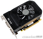
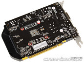
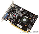
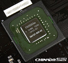
Here are the first pictures of a partner-branded GeForce GTX 750 graphics card taken apart. It reveals a couple of things - to begin with, the GM107 silicon will bring about some genuine performance per Watt improvements, despite being based on the existing 28 nm silicon fab process, and second, that cards based on the chip will be extremely cheap to build, giving NVIDIA a good chance to strengthen its position in the sub-$200 market segment. This particular card is cooled by a simple fan-heatsink that's essentially a chunk of metal with a fan latched on to it. The card relies on a simple 2+1 phase VRM, which draws power from a single 6-pin PCIe power connector. NVIDIA is expected to launch the GTX 750 and GTX 750 Ti a little later this month.
Source:
ChinaDIY


54 Comments on GTX 750 Taken Apart, Sips Power from a Single 6-pin Connector
I just lost almost all interest about Maxwell.
that's why a Fermi With a 384 cores easily beats a 768 cores on the kepler because each core on the Fermi has 2x computing power of the kepler . thanks to the shader clocks.
I Prefer performance over efficiency.
NVIDIA GM107 "Maxwell" Silicon Pictured | techPowerUp
A little info about price, if of course this end up correct.
Felbukkantak az érkező GTX 750 Ti modellek, jön a Radeon R9 280 és R7 265 | Tech2.hu
It looks like a price tag for 750Ti between 650Ti boost(before going EOL) and GTX660 if I am not mistaken(the prices exclude VAT).
1. If you're estimate that the 750 non-Ti eats 85W, how do you explain the Asus card not needing auxiliary power?
The naked PCB (from my earlier post that I linked to- and which seems to have been ignored)
The retail package
and,
2. I think it has been established that GK107 is 640 core/ 5 SMX / 128 core per SMX (information also noted in my earlier post, and publicized >>here<<)
Well.. 2 weeks or so till the (at least paper) launch. It will all become clear then.
Good puppy good boy...:rolleyes:
I have seen that picture and the strange thing about this PCB is the upper left corner where someone can see something that looks like a 6 pin connector. An early engineering sample maybe with a strangely positioned power connector?
2. Established? Not really considering that all over the place specs where talking about a 768 cores 750 and a 960 cores 750Ti, WITH gpu-z screenshots. So, those screenshots where wrong? Then it seems that whatever we knew about these cards yesterday, it is false today.
With "only" 512 cores on 750, 75W isn't really something strange. 650 with 384 cores was a 64W card. A 512 cores card with a new optimized design a couple of years latter needing less or about 75W is just something normal I think. 750Ti with "only" 640 cores I could guess it will end up close to 90W?
I personally still guessing here, nothing more. Info about these cards changes rapidly day after day.
videocardz.com/49557/exclusive-nvidia-maxwell-gm107-architecture-unveiled
The ASUS 750 is OC model but does not need a 6pin but the Gigabyte does. Just adds to the confusion.
The PCB from OP looks more inline with the Gigabyte and not the ASUS one.
None look like the Asus.
Not too tough to estimate a rough guess, though.
Scary math ahead.
(5400*128)/8 = 86.4gbps (bandwidth)
86.4/56.25 = 1.536TF (max usable shader compute)
1.536TF/960*2 = 800mhz
1150 (boost clock)/800*.16666 (special function) = ~.24
1.24*800 = 992mhz
992*960 = 1.9TF
1.9TF/(1024*2) = 930mhz (265 clockspeed is probably '925mhz' from amd, 975 AIB like 270)
1.9*56.25 = 107gbps
107*8/256 = 3348mhz (using 930mhz)
4800/3348 = 1.433
.433*.16 = ~6-7%
Obviously that number changes a little when considering slight efficiency differences (like tex units, which could bring it down a few percent), use cases (compute would be closer to the raw difference), and the core clock could be a little slower to a quite a bit faster than 930mhz, which while when faster increases performance more linearly than bw, would throw the difference bw makes off as obviously it would require more.
Yeah, it'll be faster at stock...but pretty close while being a much larger chip (even if salvage and using cheap 5ghz ram). That said, more logic + ideally low clocks (~900mhz/<5000mhz, where the process and mem controller are aimed) should keep power in check. The fact amd sells cheap and (usually) nvidia overcharges should keep the prices pretty close. It really comes down to two things:
1. How high can the mem clock on GM107, because while special function/bw voodoo of 16-17% will help at a higher clock when bw is scarce, it will be equally disproportionate scaling if bandwidth cannot feed the shaders.
2. How high can the core scale on 265? If limited to (for example) 1050mhz like 270, and the memory is crap elpida and hits (perhaps) 5300mhz, and the gm107 uses 6ghz on it's superior memory controller reaching closer to 7ghz overclocked, in theory around 1200mhz (little less on both counts) they could be roughly equal. How that plays out in power consumption considering die size, ram amount, etc is a good question.
Would that outcome surprise anyone? I bet it would not...two pretty similar-performing parts overall, even if massively different.