Tuesday, February 24th 2015

AMD's Excavator Core is Leaner, Faster, Greener
AMD gave us a technical preview of its next-generation "Carrizo" APU, which is perhaps the company's biggest design leap since "Trinity." Built on the 28 nm silicon fab process, this chip offers big energy-efficiency gains over the current-generation "Kaveri" silicon, thanks to some major under-the-hood changes.
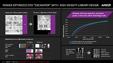
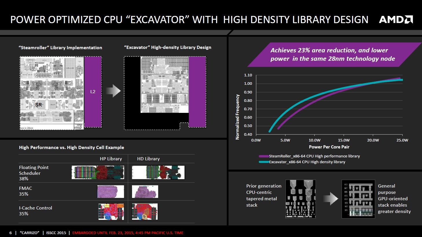
The biggest of these is the "Excavator" CPU module. 23 percent smaller in area than "Steamroller," (same 28 nm process), Excavator features a new high-density library design, which reduces die-area of the module. Most components are compacted. The floating-point scheduler is 38% smaller, fused multiply-accumulate (FMAC) units compacted by 35%, and instruction-cache controller compacted by another 35%. The "Carrizo" silicon itself uses GPU-optimized high-density metal stack, which helps with the compaction. Each "Excavator" module features two x86-64 CPU cores, which are structured much in the same way as AMD's previous three CPU core generations.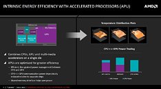
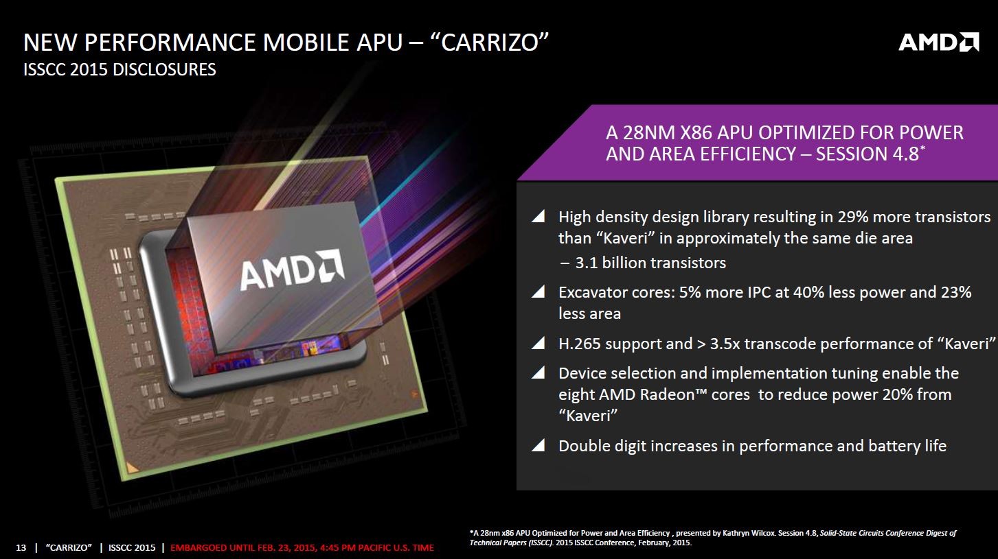
 The compaction in components doesn't necessarily translate into lower transistor-counts over "Kaveri." In fact, Carrizo features 3.1 billion transistors (Haswell-D has 1.4 billion). Other bare-metal energy optimizations include an 18% leakage reduction over previous generation, using faster RVT components, which enables 10% higher clock speeds at the same power-draw (as "Kaveri"). A new adaptive-voltage algorithm reduces CPU power draw by 19%, and iGPU power draw by 10%. AMD introduced a few new low-power states optimized for mobile devices such as >9-inch tablets and ultra-compact notebooks, which reduces overall package power draw to less than 1.5W when idling, and a little over 10W when active. In all, AMD is promising a conservative 5% IPC uplift for Excavator over Steamroller, but at a staggering 40% less power, and 23% less die-area.

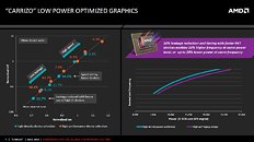
 The integrated-GPU is newer than the one featured on "Kaveri." It features 8 compute units (512 stream processors) based on Graphics CoreNext 1.3 architecture, with Mantle and DirectX 12 API support, and H.265 hardware-acceleration, with more than 3.5 times the video transcoding performance increase over "Kaveri." For notebook and tablet users, AMD is promising "double-digit percentage" improvements in battery life.
Now, if only AMD can put six of these leaner, faster, and greener "Excavator" modules onto an AM3+ chip.
The biggest of these is the "Excavator" CPU module. 23 percent smaller in area than "Steamroller," (same 28 nm process), Excavator features a new high-density library design, which reduces die-area of the module. Most components are compacted. The floating-point scheduler is 38% smaller, fused multiply-accumulate (FMAC) units compacted by 35%, and instruction-cache controller compacted by another 35%. The "Carrizo" silicon itself uses GPU-optimized high-density metal stack, which helps with the compaction. Each "Excavator" module features two x86-64 CPU cores, which are structured much in the same way as AMD's previous three CPU core generations.


Now, if only AMD can put six of these leaner, faster, and greener "Excavator" modules onto an AM3+ chip.
85 Comments on AMD's Excavator Core is Leaner, Faster, Greener
I hope also so because if they do it, I would immediately go a buy the plaform with it.
I think the next big CPU from AMD will feature a new socket and new architecture. Maybe Zen?
Which is a shame because I do NOT care about anything mobile now. /#egoismmodeswitchedon
So realistically it has no sense to compare who has what.
As long as the CPU doesn't use too much power, I don't care if it's made in 100nm techology :)
At that time, the process gap will be largely gone.
pc.watch.impress.co.jp/docs/column/kaigai/20141010_670675.html
But we have to wait for further details/proof before we decide anything.
www.semiwiki.com/forum/content/3884-who-will-lead-10nm.html
Up to 14nm Intel/20nm Fab Club they seem fairly similar enough to state one notch larger node from AMD is similar to one size smaller from Intel.
When you start getting to 14nm from the CPA, things start to get switched around. My best guess (and the numbers more-or-less follow the logic) to this is Intel will be targeting the low-power/lower-end of the voltage curve in favor of density, where-as Samsung/GF may target higher performance in effort to be more TSMC-like (notice how the CPA/TSMC essentially end in the same place). I haven't gone deep where they got their 14/16nm numbers from in relation to version of process, but it meshes pretty cleanly with TSMC shooting for roughly 10% smaller chips with 16ff+ vs earlier 16nm (which would bring them in line with the CPA 14nm process for density), and the CPA having 'early' vs 'plus' versions of the 14nm process, which the later is supposed to improve speed/power consumption (read: be more like TSMC).
Technically informed people are not buying Intel chips based on the node size. In fact Intel just delayed their 14Nm Skylake due to slow uptake on their current products and development issues with the die shrink.The process diff has little impact on actual CPU/APU performance other than primarily lower power consumption. Carrizo uses advanced power management to make significant reductions in power consumption.