News Posts matching #IPC

Return to Keyword Browsing

AMD Sampling Next-Gen Ryzen Desktop "Medusa Ridge," Sees Incremental IPC Upgrade, New cIOD

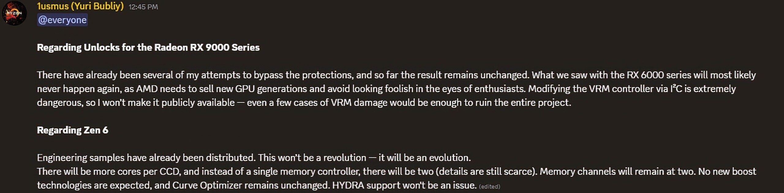
AMD is reportedly sampling its next-generation Ryzen desktop processor powered by the "Zen 6" microarchitecture, codenamed "Medusa Ridge," to close industry partners, such as platform designers and OEMs, says Yuri Bubliy, aka 1usmus, author of the Hydra tuning software, and the now-retired DRAM Calculator for Ryzen. The processor sees AMD update both the CCDs and client I/O die, he says. AMD confirmed that it is building the "Zen 6" CCD on the TSMC N2 (2 nm) node, which entered risk production earlier this year. The node is expected to be ready for mass-production of 2 nm chips later this year. The 2 nm node presents a significant jump in transistor densities from the current TSMC N4P node on which AMD builds its 8-core "Zen 5" CCD, which 1usmus and other sources say, that AMD will use to increase CPU core counts per CCD.

Sources point to the possibility of AMD increasing core counts per CCD to 12, and giving the CCD 48 MB of L3 cache. At this point we don't know if all 12 cores will be arranged in a single CCX with a monolithic slab of 48 MB L3 cache, or if there's a dual-CCX layout with 6 cores per CCX sharing 24 MB of L3 cache, each. The other big upgrade with "Medusa Ridge" is its client I/O die (cIOD). AMD is expected to build its new generation cIOD on a newer EUV node such as 5 nm N5 or 4 nm N4P, a significant upgrade from the current 6 nm N6. 1usmus says that the biggest reason for AMD to update its cIOD is the memory controller architecture. AMD is expected to give "Medusa Point" a new dual memory controller architecture. There are still two DDR5 channels per socket, but this is redesigned for increased memory speeds, letting AMD catch up with Intel in this area. As for the CPU frequency boosting technologies, such as PBO and Curve Optimizer, there are no updates expected, and 1usmus concludes that it Hydra support should be straightforward.

GPU IPC Showdown: NVIDIA Blackwell vs Ada Lovelace; AMD RDNA 4 vs RDNA 3

Instructions per clock is a metric used to define and compare CPU architecture performance usually. However, enthusiast colleagues at ComputerBase had an idea to test the IPC improvement in GPUs, comparing it across current and past generations. NVIDIA's Blackwell-based GeForce RTX 50 series faces off against the Ada Lovelace-based RTX 40 generation, while AMD's RDNA 4-powered Radeon RX 9000 lineup challenges the RDNA 3-based RX 7000 series. For NVIDIA, the test used RTX 5070 Ti and 4070 Ti SUPER, aligning ALU counts and clock speeds and treating memory bandwidth differences as negligible. For AMD, the test matched the RX 9060 XT to the RX 7600 XT, both featuring identical ALUs and GDDR6 memory. By closely matching shader counts and normalizing for clock variations, ComputerBase isolates IPC improvements from other hardware enhancements. In rasterized rendering tests across 19 popular titles, NVIDIA's Blackwell architecture delivered an average IPC advantage of just 1% over the older Ada Lovelace.

This difference could easily be attributed to normal benchmark variance. Ray tracing and path tracing benchmarks showed no significant IPC uplift, leaving the latest generation essentially on par with its predecessor when normalized for clock and unit count. AMD's RDNA 4, by contrast, exhibited a substantial IPC leap. Rasterized performance improved by around 20% compared to RDNA 3, while ray-traced workloads enjoyed a roughly 31% gain. Path tracing results were even more extreme, with RDNA 4 delivering nearly twice the FPS, a 100% increase over its predecessor. These findings suggest that NVIDIA's performance improvements primarily stem from higher clock speeds, increased execution unit counts, and enhanced features. AMD's RDNA 4 represents a significant architectural advance, marking its most notable IPC gain since the original RDNA launch.

BCM Intros RX880W microATX Industrial Motherboards with Support for Intel Core Ultra 9 CPUs

The BCM RX880W is a new microATX motherboard built on Intel's latest Core Ultra platform, formerly known as Arrow Lake-S/Arrow Lake-S Refresh, pairing the Intel W880 chipset with the LGA1851 socket to support the 15th Gen Intel Core Ultra processors (Series 2). This board is designed to deliver cutting-edge performance while retaining robust legacy support, making it ideal for hardware and system engineers in the fields of medical & healthcare, industrial & automation, smart retail, digital signage, intelligent Kiosk, Edge AI server, security, and electronics distributors seeking next-generation solutions.

RX880W microATX New Design Features for Edge AI Computing and Compact Storage Servers
High-Performance with AI enabled CPU Support:
  • LGA1851 socket supports Intel's latest Core Ultra 5/7/9 processors (Series 2), up to 125 W TDP
  • Dual SlimSAS Connectors - High-Speed Storage in Compact Systems
    • The RX880W integrates two SlimSAS (SFF-8654) connectors—a standout feature rarely seen on industrial Micro ATX motherboards. Each SlimSAS supports PCIe Gen 4 x4, enabling flexible, high-bandwidth storage options ideal for dense, compact edge and storage platforms.

MSI Teases EdgeXpert MS-C931 - an NVIDIA DGX Spark-based Desktop AI Supercomputer

MSI IPC, a global leader in industrial computing and AI-driven solutions, is set to unveil its latest innovations at COMPUTEX 2025, held from May 20 to 23 at the Taipei Nangang Exhibition Center. Visitors can explore MSI IPC's cutting-edge technologies at Booth J0506, Hall 1, 1F.

Introducing the EdgeXpert MS-C931: A Desktop AI Supercomputer
MSI IPC will unveil the EdgeXpert MS-C931, a desktop AI supercomputer built on the NVIDIA DGX Spark platform. Powered by the NVIDIA GB10 Grace Blackwell Superchip, the EdgeXpert MS-C931 delivers 1,000 AI TOPS FP4 performance, equipped with high-speed ConnectX 7 networking, 128 GB unified memory, and support for large language models. Designed for AI developers and researchers, it is ideal for applications in education, finance, and healthcare industries.

Biostar Launches EdgeComp MS-J6412 IPC for Edge Computing Applications

BIOSTAR, a leading manufacturer of IPC solutions, motherboards, graphics cards, and storage devices, is excited to introduce the EdgeComp MS-J6412 industrial PC, a powerful new addition to its EdgeComp series built specifically for industrial automation and edge computing applications.

Designed to excel in demanding industrial settings, EdgeComp MS-J6412 combines powerful performance, energy efficiency, and versatile connectivity in a compact, fanless design. Powered by the Intel Elkhart Lake J6412 SoC, a quad-core processor with speeds up to 2.6 GHz and an ultra-low 10 W TDP, the system ensures stable, round-the-clock operation with minimal heat generation and silent performance. Its embedded architecture makes it ideally suited for space-limited and noise-sensitive environments where reliability is paramount.

MSI IPC Showcases AI & Edge Solutions with Intel Arrow Lake at Japan IT Week Spring 2025

MSI IPC, a leading provider of industrial computing solutions, is set to exhibit at Japan IT Week Spring 2025, held from April 23-25 at Tokyo Big Sight, Booth East Hall 3 #21-2. The company will showcase its latest innovations in AI computing, embedded systems, and edge intelligence, designed for smart manufacturing, medical, transportation, and industrial applications.

Explore the Future of Industrial Computing
MSI IPC will host a static demo featuring Intel Twin Lake, Raptor Lake, and Arrow Lake, allowing attendees to experience next-gen performance and AI acceleration. Key platforms include:
  • MS-CF20 ATX (W880 chipset)- Built for high-performance workloads with expandability for industrial applications.
  • MS-CF23 Mini-ITX (H810 chipset) - Compact yet powerful, ideal for space-sensitive deployments.
  • MS-C927 Embedded Box PC (Arrow Lake-U & Meteor Lake-U) - Fanless, wide-temp system for industrial and embedded environments.

MSI IPC Introduces High-Performance ATX Motherboard MS-CF05, V2.0 for Industrial and Embedded Applications

MSI IPC, a global leader in industrial computing solutions, proudly unveils the MS-CF05, V2.0, a high-performance ATX motherboard engineered for industrial automation, edge computing, and embedded applications. Designed to support 14th, 13th, and 12th Gen Intel Core, Pentium, and Celeron processors, the MS-CF05, V2.0 delivers exceptional computing power, scalability, and I/O flexibility, including a PCI slot for legacy support, making it ideal for modern industrial needs.

MSI IPC Showcases Cutting-Edge Edge AI Computing Solutions at Embedded World 2025

MSI IPC, a global leader in computing and AI-driven solutions, is set to unveil its latest Edge AI Computing innovations at Booth No. 1-389, Embedded World 2025 in Nuremberg, Germany. Powered by the latest Intel platform, MSI's cutting-edge technologies will drive advancements in automation, digital signage management, and AI-driven customer interactions.

Several MSI's partners, including Alptech, Spo-comm, Spectra, and Elmark, are joining this event to showcase their cutting-edge solutions powered by MSI IPC products. Their demonstrations will feature a diverse range of applications, including 4U rackmount systems, Panel PCs (PPC), and KIOSK solutions, highlighting the versatility and performance of MSI's industrial computing technology in various sectors.

AMD Discusses EPYC's "No Compromise" Driving of Performance and Efficiency

One of the main pillars that vendors of Arm-based processors often cite as a competitive advantage versus x86 processors is a keen focus on energy efficiency and predictability of performance. In the quest for higher efficiency and performance, Arm vendors have largely designed out the ability to operate on multiple threads concurrently—something that most enterprise-class CPUs have enabled for years under the technology description of "SMT"—which was also created in the name of enabling performance and efficiency benefits.

Arm vendors often claim that SMT brings security risks, creates performance unpredictability from shared resource contention and drives added cost and energy needed to implement SMT. Interestingly, Arm does support multi-threading in its Neoverse E1-class processor family for embedded uses such as automotive. Given these incongruities, this blog intends to provide a bit more clarity to help customers assess what attributes of performance and efficiency really bring them value for their critical workloads.

Intel Core Ultra 300 Series "Panther Lake-H" to Come with 64 W PL2 Power Configuration

Thanks to a well-known industry leaker, Jaykihn, Intel's Panther Lake-H processor family, built on the 18A process node, features three distinct configurations, with several power profiles for each case. The flagship model combines four "Cougar Cove" P-cores, eight "Skymont" E-cores, and four LPE cores alongside a 12-core Xe3 "Celestial" GPU. This variant supports LPDDR5X memory exclusively and delivers 180 TOPS of computational power for local AI workloads, operating at 25 W PL1 (base) and 64 W PL2 (turbo) power levels. Secondary configurations include a 4P+8E+4LP+4Xe3 model and a 4P+0E+4LP+4Xe3 variant, both rated at 100 TOPS and supporting both LPDDR5X and DDR5 memory.

The entry-level model operates at 15 W PL1 with 44 W PL2 in baseline mode, scaling to 25 W PL1 and 55 W PL2 in performance mode. All variants feature Thunderbolt 4 connectivity, with high-end models incorporating expanded PCIe 5.0 lane configurations. The integrated Xe3 graphics architecture scales from four to 12 cores across the product stack, with the top SKU eliminating DDR5 compatibility in favor of LPDDR5X optimization. The Panther Lake processor family is slated for launch within the latter half of 2025, and it will be the company's leading 18A product. As a "Lunar Lake" successor, Panther Lake will deliver improved IPC and optimization for new cores in the same device form-factor like laptops, ultrabooks, and handhelds.

Biostar and DEEPX Showcase Advanced Edge AI Solutions at CES 2025

BIOSTAR, a leading manufacturer of Edge AI embedded computers, IPC solutions motherboards, graphics cards, and PC peripherals, is excited to announce x86 Edge AI platform showcase at CES 2025. Scheduled to take place from January 7 to 10 in Las Vegas, Nevada, USA, BIOSTAR, in partnership with DEEPX, an AI semiconductor company from South Korea, will showcase cutting-edge x86 Edge AI solutions at DEEPX's booth (#9045) in the North Hall of the Las Vegas Convention Center.

DEEPX is a pioneering company in on-device AI. It develops advanced AI semiconductors that optimize performance, reduce power consumption, and enhance cost efficiency across various industries, including smart camera modules, smart mobility, smart factories, consumer electronics, smart cities, surveillance systems, and AI servers. Building upon their successful collaborations, BIOSTAR and DEEPX set to unveil their latest joint innovations at CES 2025, further enhancing their prominence in the industrial computing ecosystem.

InWin Introduces New Server & IPC Equipment at CES 2025

InWin has showcased several new server chassis models at CES—these new introductions form part of the company's efforts to expand regional IPC, server, and systems assembly operations going into 2025. New manufacturing facilities in the USA and Malaysia were brought online last year, and new products have sprung forth. TechPowerUp staffers were impressed by InWin's RG650B model—this cavernous rackmount GPU server has been designed with AI and HPC applications in mind. Its 6.5U dual-chamber design is divided into two sections with optimized and independent heat dissipation systems—GPU accelerators are destined for the 4.5U space, while the motherboard and CPUs go into the 2U chamber.

The RG650B's front section is dominated by the nine pre-installed hot swappable 80 x 30 mm (12,000 RPM max. rated) PWM fans. This array should provide plenty of cooling for any contained hardware; these components will be powered by an 80 Plus Titanium CRPS 3200 W PSU (with four 12V-2x6 pin connectors). InWin's spec sheet states that their RG650B supports 18 FHFL PCI-Express slots with four PCI-Express riser cables—granting plenty of potential for the installation of add-in boards.

Intel Nx50 Series "Twin Lake" Pure E-core Processor Line Powered by "Skymont" Surfaces

"Twin Lake" is codename for a line of low-power x86-64 processors by Intel, which succeed the Core i3 N-series and N200 series "Alder Lake-N" processors. These non-socketed (BGA) chips power a wide range of devices from entry level notebooks and mini PCs to consumer NAS servers, and other embedded applications. The chips feature only E-cores. While "Alder Lake-N" used "Gracemont" cores, "Twin Lake" uses the swanky new "Skymont" cores, which serve as E-cores in "Lunar Lake" and "Arrow Lake" hybrid processors. "Skymont" cores feature massive IPC and clock-speed gains over "Gracemont," of nearly 50%, which pulls up their performance levels to match the "Golden Cove" and "Raptor Cove" P-cores of "Alder Lake" and "Raptor Lake," although these cores can't boost up to 5.00 GHz. We got the first name-drop of "Twin Lake" way back in May 2024. Jaykihn leaked what the processor lineup could look like.

The "Twin Lake" silicon features two "Skymont" E-core clusters sharing an L3 cache. At this point, the sizes of the shared L2 caches of the E-core clusters, and the size of the shared L3 cache are not known. On "Alder Lake-N," each "Gracemont" cluster features 2 MB of L2 cache, and the two clusters share a 6 MB L3 cache. The silicon also features an iGPU based on what is very likely the Xe-LPG graphics architecture, with four Xe cores worth 32 execution units (EU). The series is led by the Intel N355. This chip maxes out the "Twin Lake" silicon, enabling both "Skymont" clusters, for an 8-core/8-thread CPU configuration. The CPU comes with a base frequency of 3.00 GHz, and boosts up to 3.90 GHz. The chip comes with a configurable TDP of 9 W and 15 W. It comes with a maxed out iGPU, with all 32 EU being enabled, and a graphics frequency of 1.35 GHz.

Intel "Panther Lake" Confirmed on 18A Node, Powering-On With ES0 Silicon Revision

During Barclays 22nd Annual Global Technology Conference, Intel was a guest and two of the interim company co-CEOs Michelle Johnston Holthaus and David Zinsner gave a little update on the state of affairs at Intel. One of the most interesting aspects of the talk was Intel's upcoming "Panther Lake" processor—a direct successor to Intel Core Ultra 200S "Arrow Lake-H" mobile processors. The company confirmed that Panther Lake would utilize an Intel 18A node and that a few select customers have powered on Panther Lake on the E0 engineering sample chip. "Now we are using Intel Foundry for Panther Lake, which is our 2025 product, which will land on 18A. And this is the first time that we're customer zero in a long time on an Intel process," said interim co-CEO Michelle Johnston Holthaus, adding, "But just to give some assurances, on Panther Lake, we have our ES0 samples out with customers. We have eight customers that have powered on, which gives you just kind of an idea that the health of the silicon is good and the health of the Foundry is good."

While we don't know what ES0 means for Intel internally, we can assume that it is one of the first engineering samples on the 18A. The "ES" moniker usually refers to engineering samples, and zero after it could be the first design iteration. For reference, Intel's "Panther Lake-H" will reportedly have up to 18 cores: 6 P-cores, 8 E-cores, and 4 LP cores. The design brings back low-power island E-cores in the SoC tile. The P-cores use "Cougar Cove," which should have a higher IPC than "Lion Cove," while keeping the existing "Skymont" E-cores. The SoC tile may move from Arrow Lake's 6 nm to a newer process to fit the LP cores and an updated NPU. The iGPU is said to use the Xe3 "Celestial" architecture. With Arrow Lake-H launching in early 2025, Panther Lake-H likely won't arrive until 2026.

AMD Ryzen 7 9800X3D Comes with 120W TDP, 5.20 GHz Boost, All Specs Leaked

Specifications of the upcoming AMD Ryzen 7 9800X3D processor were leaked to the web by a Geizhals listing. The chip comes with a processor base frequency of 4.70 GHz, and a maximum boost frequency of 5.20 GHz. The base frequency of 4.70 GHz is a significant increase from the 4.20 GHz of the current 7800X3D, while the maximum boost frequency has moved up a couple of notches from the 5.05 GHz of the 7800X3D. The TDP of the processor is set at 120 W, same as the 7800X3D, and higher than the 105 W revised-spec cTDP of the non-X3D Ryzen 7 9700X.

The specs sheet also confirms that the 3D V-cache size is unchanged generationally. The stacked 3D V-cache die adds 64 MB to the on-die 32 MB L3 cache, which is exposed to software as a 96 MB contiguously addressable L3 cache. The per-core L2 cache size remains 1 MB per core. The biggest contributor to generational gaming performance increases will rest on the increase in frequencies, the new "Zen 5" microarchitecture and any IPC improvements on offer, plus L3 cache performance improvements AMD introduced with "Zen 5." We recently reported a spectacular theory that AMD has designed the 9800X3D such that the stacked 3D V-cache is positioned below the 8-core CPU complex die chiplet, and not above it, which should significantly improve thermals, and clock speeds.

AMD Sets Up Press Event for Ryzen 7 9800X3D Launch

AMD China has set up a press event to launch its new Ryzen 7 9800X3D "Zen 5" processor with 3D V-cache. The company is sending out invitations like the one pictured below to the Chinese tech press and select PC enthusiasts. The event is slated to take place in Zhuhai, and spans October 23 and 24, which could mean that the company has set up an experience zone, where visitors can take gaming desktops powered by the 9800X3D for a spin with popular game titles. It won't surprise us if AMD has at least an online press event planned around this time for the rest of the world.

The Ryzen 7 9800X3D is widely expected to extend AMD's lead with gaming performance. In first-party gaming benchmarks put out by Intel for its upcoming Core Ultra 9 285K "Arrow Lake" processor, the new chip is shown within 3% of the Core i9-14900K, which the current Ryzen 7 7800X3D beats, and the 9800X3D can only push the gaming performance envelope further from here. If it's not the higher IPC of "Zen 5," then it could be the alleged 5.20 GHz all-core boost frequency for the 9800X3D. The Ryzen 7 9800X3D is expected to go on sale in the first week of November 2024.

AMD Launches 5th Gen AMD EPYC CPUs, Maintaining Leadership Performance and Features for the Modern Data Center

AMD (NASDAQ: AMD) today announced the availability of the 5th Gen AMD EPYC processors, formerly codenamed "Turin," the world's best server CPU for enterprise, AI and cloud. Using the "Zen 5" core architecture, compatible with the broadly deployed SP5 platform and offering a broad range of core counts spanning from 8 to 192, the AMD EPYC 9005 Series processors extend the record-breaking performance and energy efficiency of the previous generations with the top of stack 192 core CPU delivering up to 2.7X the performance compared to the competition.

New to the AMD EPYC 9005 Series CPUs is the 64 core AMD EPYC 9575F, tailor made for GPU powered AI solutions that need the ultimate in host CPU capabilities. Boosting up to 5 GHz, compared to the 3.8 GHz processor of the competition, it provides up to 28% faster processing needed to keep GPUs fed with data for demanding AI workloads.

AAEON Launch Multi-Touch Panel PCs Powered by Intel Processor N-series

Leading IPC provider AAEON today announced the release of two new Panel PCs: the ACP-2106, which features a 10" WXGA screen, and the ACP-2076, equipped with a 7" WSVGA Projected Capacitive Multi-Touch screen. Compared to its previous Panel PC offerings, both the ACP-2106 and ACP-2076 offer substantial improvements in processing power, with a choice of either the Intel Processor N50 or Intel Processor N97 CPU. Moreover, both new additions to the range support up to 32 GB of DDR5, compared to the 8 GB of DDR3L offered by the previous generation. With these improvements, the ACP-2106 and ACP-2076 are clearly designed for use in more advanced and taxing industrial and commercial applications, with retail and industrial automation thought to be primary target markets.

The ACP-2076 grants users a 7" display with 1024 x 600 resolution, while the ACP-2106's 10" screen offers a slightly higher resolution of 1280 x 800. Both PCs are also equipped with an HDMI 1.4b port, making them suitable for applications that require dual-display capabilities, such as smart kiosks. Both models also provide wide viewing angles and high brightness levels, with the ACP-2076 achieving 320 cd/m² and the ACP-2106 reaching 300 cd/m², ensuring consistent visibility in a variety of environments.

MSI Unveils MS-C906 Ultra-Low-Power Fanless Box IPC for Edge AI Applications

MSI, a global leader in AI and advanced computing solutions, proudly announces the launch of the MS-C906, a compact-size Box PC powered by the Intel 13th Gen Raptor Lake-P U Series Processor. Designed for ultra-low-power fanless operation, the MS-C906 is ideal for edge AI applications, offering unparalleled performance and reliability.

Key Features:
  • High Performance: Supports up to 32 GB of DDR5 5200 MHz RAM and features quadruple independent HDMI displays, perfect for versatile visual output in various industrial and commercial environments.
  • Robust Connectivity: Equipped with four Intel 2.5GbE LAN ports, ensuring robust network connectivity. M.2 and SATA interfaces provide ample storage options.

Intel Granite Rapids SKUs Detailed With Up To 128 Cores and 500 W TDP

The newest leak from X (formerly Twitter) has detailed five Intel Granite Rapids SKUs, including the 6980P, 6979P, 6972P, 6952P, and the 6960P. Featuring up to 128 CPU cores and up to 504 MB of cache, these show that Intel Granite Rapids will double the amount of cores compared to the Emerald Rapids SKUs.

The newest leak coming from Jaykihn over at X, following the previous leak that detailed the most powerful SKU. The 6980P will pack 128 cores, pack 504 MB of cache, have a 2.0 GHz base frequency and a massive 500 W TDP rating. The rest of the SKUs have lower core count, ending with the 6960P, which comes with 72 cores, 432 MB of cache, but also a higher 2.7 GHz base frequency.

AMD Strix Point SoC Reintroduces Dual-CCX CPU, Other Interesting Silicon Details Revealed

Since its reveal last week, we got a slightly more technical deep-dive from AMD on its two upcoming processors—the "Strix Point" silicon powering its Ryzen AI 300 series mobile processors; and the "Granite Ridge" chiplet MCM powering its Ryzen 9000 desktop processors. We present a closer look into the "Strix Point" SoC in this article. It turns out that "Strix Point" takes a significantly different approach to heterogeneous multicore than "Phoenix 2." AMD gave us a close look at how this works. AMD built the "Strix Point" monolithic silicon on the TSMC N4P foundry node, with a die-area of around 232 mm².

The "Strix Point" silicon sees the company's Infinity Fabric interconnect as its omnipresent ether. This is a point-to-point interconnect, unlike the ringbus on some Intel processors. The main compute machinery on the "Strix Point" SoC are its two CPU compute complexes (CCX), each with a 32b (read)/16b (write) per cycle data-path to the fabric. The concept of CCX makes a comeback with "Strix Point" after nearly two generations of "Zen." The first CCX contains the chip's four full-sized "Zen 5" CPU cores, which share a 16 MB L3 cache among themselves. The second CCX contains the chip's eight "Zen 5c" cores that share a smaller 8 MB L3 cache. Each of the 12 cores has a 1 MB dedicated L2 cache.

CPU-Z Screenshot of Alleged Intel Core Ultra 9 285K "Arrow Lake" ES Surfaces, Confirms Intel 4 Process

A CPU-Z screenshot of an alleged Intel Core Ultra 9 285K "Arrow Lake-S" desktop processor engineering sample is doing rounds on social media, thanks to wxnod. CPU-Z identifies the chip with an Intel Core Ultra case badge with the deep shade of blue associated with the Core Ultra 9 brand extension, which hints at this being the top Core Ultra 9 285K processor model, we know it's the "K" or "KF" SKU looking at its processor base power reading of 125 W. The chip is built in the upcoming Intel Socket LGA1851. CPU-Z displays the process node as 7 nm, which corresponds with the Intel 4 foundry node.

Intel is using the same Intel 4 foundry node for "Arrow Lake-S" as the compute tile of its "Meteor Lake" processor. Intel 4 offers power efficiency and performance comparable to 4 nm nodes from TSMC, although it is physically a 7 nm node. Likewise, the Intel 3 node is physically 5 nm. If you recall, the main logic tile of "Lunar Lake" is being built on the TSMC N3P (3 nm) node. This means that Intel is really gunning for performance/Watt with "Lunar Lake," to get as close to the Apple M3 Pro as possible.

MSI Unveils MS-C907 Embedded Box IPC

MSI is excited to introduce the MS-C907, a robust and versatile embedded Box IPC designed to meet the demanding requirements of various industries. Beyond its suitability for the chemical industry, the MS-C907 is ideal for applications in factory automation, transportation, digital signage and retail.

Meeting the Needs of Multiple Industries
The MS-C907 offers robust performance, extensive connectivity, and durable design, making it an ideal solution for a wide range of industrial applications. Whether it's automating factory processes, powering digital signage, or managing smart building systems, the MS-C907 provides the reliability and efficiency needed for continuous operation.

Intel Core Ultra 200 "Arrow Lake-S" Desktop Processor Core Configurations Surface

Intel is preparing a complete refresh of its desktop platform this year, with the introduction of the Core Ultra 200 series processors based on the "Arrow Lake" microarchitecture. The company skipped a desktop processor based on "Meteor Lake," probably because it didn't meet the desired multithreaded performance targets for Intel as it maxed out at 6P+8E+2LP, forcing Intel to come up with the 14th Gen Core "Raptor Lake Refresh" generation to see it through 2H-2023 and at least three quarters of 2024. The company, in all likelihood, will launch the new "Arrow Lake-S" Core Ultra 200 series toward late-Q3 or early-Q4 2024 (September-October). The first wave will include the overclocker-friendly K- and KF SKUs, alongside motherboards based on the top Intel Z890 chipset. 2025 will see the series ramp to more affordable processor models, and mainstream chipsets, such as the B860. These processors require a new motherboard, as Intel is introducing the new Socket LGA1851 with them.

Core configurations of the "Arrow Lake-S" chip surfaced on the web thanks to Jaykihn, a reliable source with Intel leaks. In its maximum configuration, the chip is confirmed to feature 8 P-cores, and 16 E-cores. There are no low-power island E-cores. Each of the 8 P-cores is a "Lion Cove" featuring 3 MB of dedicated L2 cache; while each the E-cores are "Skymont," arranged in 4-core modules that share 4 MB L2 caches among them. Intel claims that the "Lion Cove" P-core offers a 14% IPC increase over the "Redwood Cove" P-core powering "Meteor Lake," which in turn had either equal or a 1% IPC regression compared to "Raptor Cove." This would put "Lion Cove" at a 13-14% IPC advantage over the "Raptor Cove" cores. It's important to note here, that the "Lion Cove" P-cores lack HyperThreading, so Intel will be banking heavily on the "Skymont" E-cores to shore up generational multithreaded performance increase. "Skymont" was a show-stopper at Intel's Computex event, with a nearly 50% IPC gain over previous generations of Intel E-cores, which puts it at par with the "Raptor Cove" cores in single-thread performance.

Intel Arc Xe2 "Battlemage" Discrete GPUs Made on TSMC 4 nm Process

Intel has reportedly chosen the TSMC 4 nm EUV foundry node for its next generation Arc Xe2 discrete GPUs based on the "Battlemage" graphics architecture. This would mark a generational upgrade from the Arc "Alchemist" family, which Intel built on the TSMC 6 nm DUV process. The TSMC N4 node offers significant increases in transistor densities, performance, and power efficiency over the N6, which is allowing Intel to nearly double the Xe cores on its largest "Battlemage" variant in numerical terms. This, coupled with increased IPC, clock speeds, and other features, should make the "Battlemage" contemporary against today's AMD RDNA 3 and NVIDIA Ada gaming GPUs. Interestingly, TSMC N4 isn't the most advanced foundry node that the Xe2 "Battlemage" is being built on. The iGPU powering Intel's Core Ultra 200V "Lunar Lake" processor is part of its Compute tile, which Intel is building on the more advanced TSMC N3 (3 nm) node.
Return to Keyword Browsing
Jul 14th, 2025 22:46 CDT change timezone

New Forum Posts

Popular Reviews

TPU on YouTube

Controversial News Posts