News Posts matching #IPC

Return to Keyword Browsing

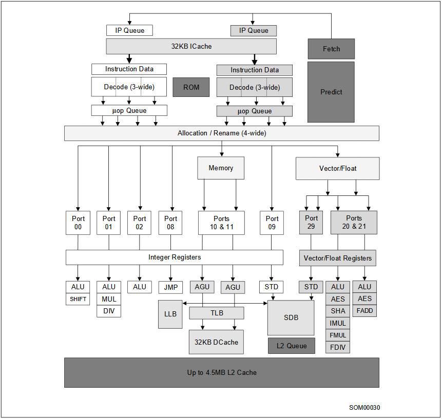
First Signs of AMD Zen 3 "Vermeer" CPUs Surface, Ryzen 7 5800X Tested

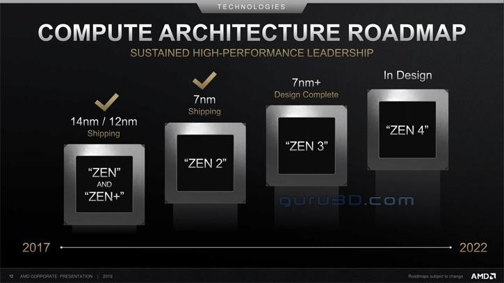
AMD is preparing to launch the new iteration of desktop CPUs based on the latest Zen 3 core, codenamed Vermeer. On October 8th, AMD will hold the presentation and again deliver the latest technological advancements to its desktop platform. The latest generation of CPUs will be branded as a part of 5000 series, bypassing the 4000 series naming scheme which should follow, given that the prior generation was labeled as 3000 series of processors. Nonetheless, AMD is going to bring a new Zen 3 core with its processors, which should bring modest IPC gains. It will be manufactured on TSMC's 7 nm+ manufacturing node, which offers a further improvement to power efficiency and transistor density.

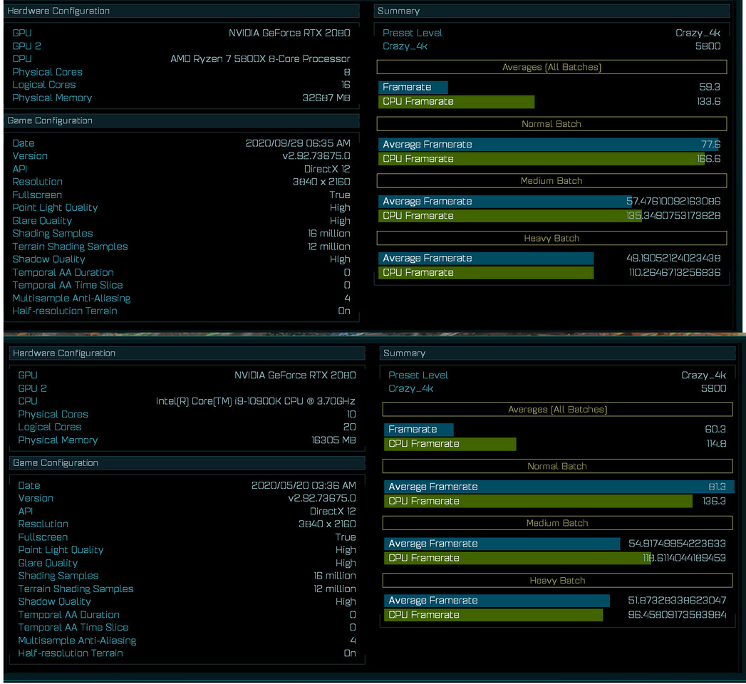
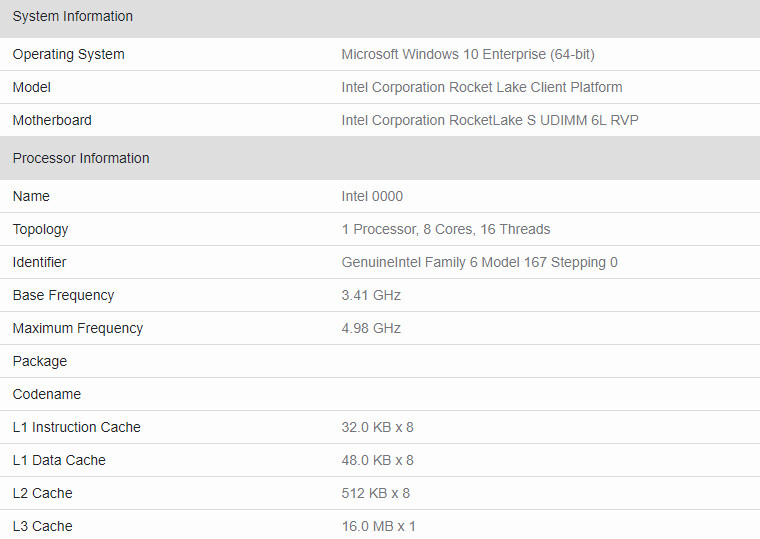
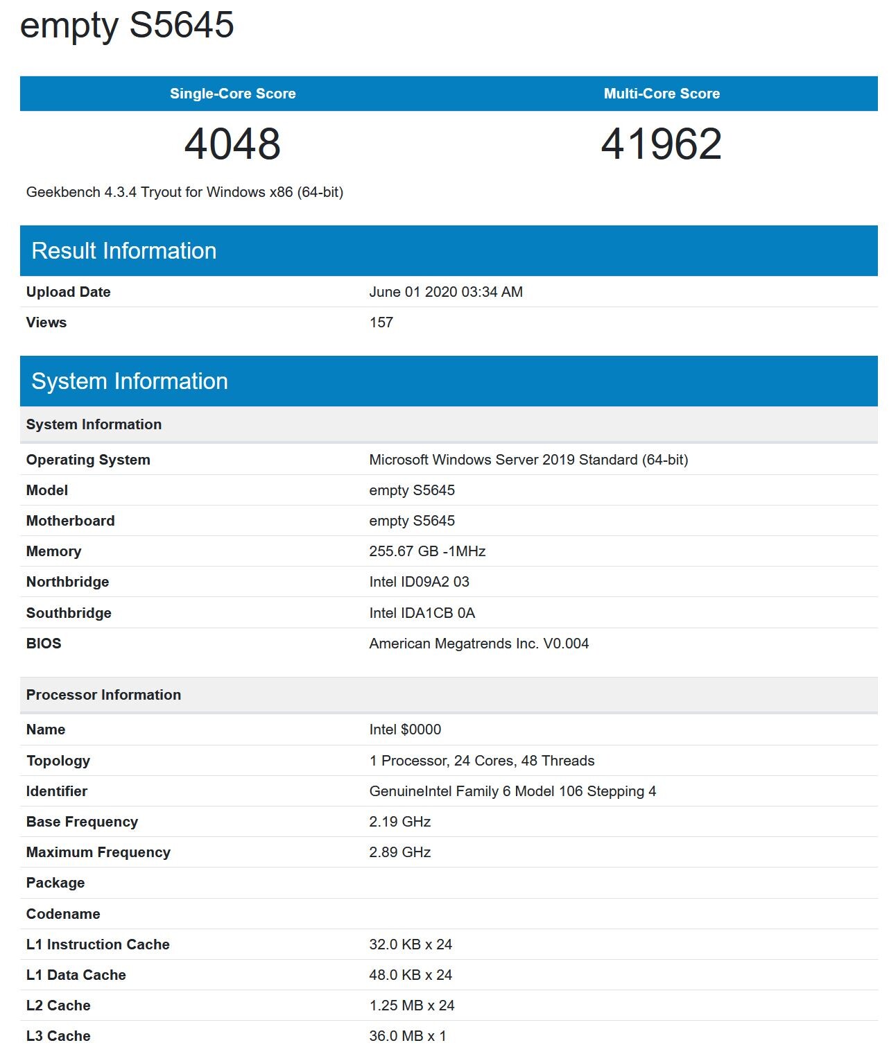
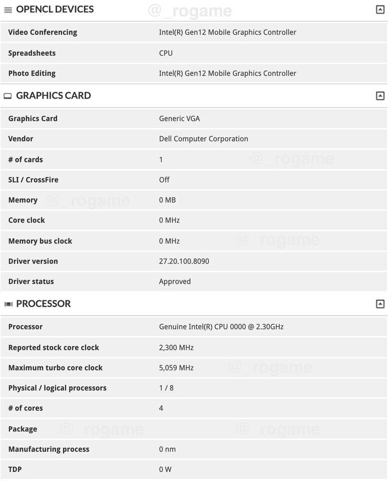
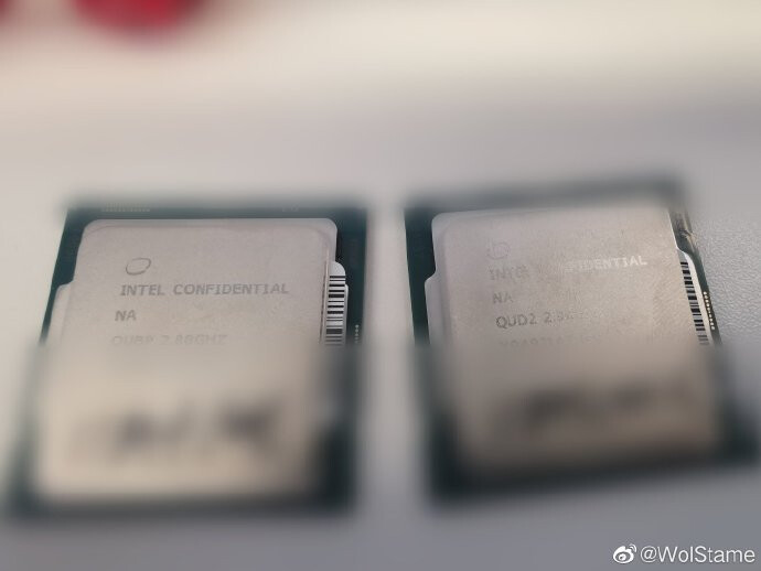
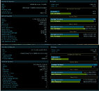
Today, we have gotten the first benchmark of AMD's upcoming Ryzen 7 5800X CPU. Thanks to the popular hardware leaker, TUP APISAK, we have the first benchmark of the new Vermeer processor, compared to Intel's latest and greatest - Core i9-10900K. The AMD processor is an eight-core, sixteen threaded model compared to the 10C/20T Intel processor. While we do not know the final clocks of the AMD CPU, we could assume that the engineering sample was used and we could see an even higher performance. Below you can see the performance of the CPU and how it compares to Intel. By the numbers shown, we can expect AMD to possibly be a new gaming king, as the numbers are very close to Intel. The average batch result for the Ryzen 7 5800X was 59.3 FPS and when it comes to CPU frames it managed to score 133.6 FPS. Intel's best managed to average 60.3 FPS and 114.8 FPS from the CPU framerates. Both systems were tested with NVIDIA's GeForce RTX 2080 GPUs.

Arm Announces Next-Generation Neoverse V1 and N2 Cores

Ten years ago, Arm set its sights on deploying its compute-efficient technology in the data center with a vision towards a changing landscape that would require a new approach to infrastructure compute.

That decade-long effort to lay the groundwork for a more efficient infrastructure was realized when we announced Arm Neoverse, a new compute platform that would deliver 30% year-over-year performance improvements through 2021. The unveiling of our first two platforms, Neoverse N1 and E1, was significant and important. Not only because Neoverse N1 shattered our performance target by nearly 2x to deliver 60% more performance when compared to Arm's Cortex-A72 CPU, but because we were beginning to see real demand for more choice and flexibility in this rapidly evolving space.

Intel Xeon Scalable "Ice Lake-SP" 28-core Die Detailed at Hot Chips - 18% IPC Increase

Intel in the opening presentation of the Hot Chips 32 virtual conference detailed its next-generation Xeon Scalable "Ice Lake-SP" enterprise processor. Built on the company's 10 nm silicon fabrication process, "Ice Lake-SP" sees the first non-client and non-mobile deployment of the company's new "Sunny Cove" CPU core that introduces higher IPC than the "Skylake" core that's been powering Intel microarchitectures since 2015. While the "Sunny Cove" core itself is largely unchanged from its implementation in 10th Gen Core "Ice Lake-U" mobile processors, it conforms to the cache hierarchy and tile silicon topology of Intel's enterprise chips.

The "Ice Lake-SP" die Intel talked about in its Hot Chips 32 presentation had 28 cores. The "Sunny Cove" CPU core is configured with the same 48 KB L1D cache as its client-segment implementation, but a much larger 1280 KB (1.25 MB) dedicated L2 cache. The core also receives a second fused multiply/add (FMA-512) unit, which the client-segment implementation lacks. It also receives a handful new instruction sets exclusive to the enterprise segment, including AVX-512 VPMADD52, Vector-AES, Vector Carry-less Multiply, GFNI, SHA-NI, Vector POPCNT, Bit Shuffle, and Vector BMI. In one of the slides, Intel also detailed the performance uplifts from the new instructions compared to "Cascade Lake-SP".

AMD "Cezanne" APU Spotted: Retains Renoir's iGPU, Updates CPU to "Zen 3"

AMD's 5th Generation Ryzen "Cezanne" APU sprung up on SiSoft SANDRA database, with big hints as to the areas where the company could innovate next. Apparently, "Cezanne" is a very similar silicon to "Renoir." It appears to feature the same iGPU solution, based on the "Vega" architecture. We're now learning that the iGPU even has the same core configuration, with up to 512 stream processors, and a likely bump in iGPU engine clocks over the Ryzen 4000 "Renoir" chips.

Much of the innovation is with the CPU component. Although the CPU core count is not yet known, the company is deploying its "Zen 3" microarchitecture, which sees all cores on the silicon sharing a large common slab of L3 cache. The "Vega" based iGPU should still perform better than the solution on "Renoir," as it's assisted by higher engine clocks, and possibly a higher IPC CPU component. In the SANDRA screenshot, the iGPU was shown bearing 1.85 GHz engine clocks, which amounts to a 100 MHz speed-bump compared to the engine clocks of the Ryzen 4000H and 4000U.

Intel "Tiger Lake" Launch Slated for September 2, Raja Koduri to Update Xe Progress Mid-August

Intel will launch its 11th Generation Core "Tiger Lake" mobile processors on September 2. The company sent out invites to a "virtual event" to be held on that date, which will be webcast to the public. On that day, several major notebook manufacturers are expected to unveil their next-generation devices based on the new processors. "Tiger Lake" is an important product launch for Intel as it marks the commercial debut of its ambitious Xe graphics architecture as the chip's Gen12 integrated graphics solution. In related news, Intel's chief architect for Xe, Raja Koduri, is expected to lead a webcast on August 13, where he will provide an update on his team's work.

The processors also debut the "Willow Cove" CPU cores that offer increased IPC over current "Sunny Cove" and "Skylake" cores, which will play a big role in closing the performance gap against the 8-core "Zen 2" processors by AMD based on the "Renoir" silicon. "Tiger Lake" is also expected to be one of the final front-line mobile processors by Intel to feature only one kind of CPU cores, as the company is expected to go big on Hybrid core technology with its future microarchitectures.

Intel to Clock "Rocket Lake-S" High, Evidence of an ES with 5.00 GHz Boost

Intel's 11th Generation Core "Rocket Lake-S" desktop processors in the LGA1200 package could come with clock speeds that are of the norm these days. Intel appears unwilling to dial down clock speeds in the wake of increased IPC with the new generation "Cypress Cove" CPU cores that drive these processors. Twitter handle "leakbench," which tracks interesting Geekbench results, fished out a database listing for a "Rocket Lake-S" engineering sample with clock speeds of 3.40 GHz base, and 5.00 GHz boost.

The listing has all the telltale signs of "Cypress Cove," such as 48 KB L1D cache, 512 KB per core L2 cache, and 16 MB shared L3 cache for this 8-core/16-thread chip. "Cypress Cove" is rumored to be to be a back-port of Intel's "Willow Cove" CPU core design from its original 10 nm+ node to the 14 nm++. VideoCardz compared this "Rocket Lake-S" ES benchmark result to that of a retail Core i7-10700K, and found its single-threaded performance to be roughly 6.35 percent higher despite a 200 MHz clock-speed deficit, although for some reason, its multi-threaded performance is trailing by over 15 percent.

Intel Rocket Lake CPUs Will Bring up to 10% IPC Improvement and 5 GHz Clocks

Intel is struggling with its node development and it looks like next-generation consumer systems are going to be stuck on 14 nm for a bit more. Preparing for that, Intel will finally break free from Skylake-based architectures and launch something new. The replacement for the current Comet Lake generation is set to be called Rocket Lake and today we have obtained some more information about it. Thanks to popular hardware leaker rogame (_rogame), we know a few stuff about Rocket Lake. Starting off, it is known that Rocket Lake features the backport of 10 nm Willow Cove core, called Cypress Cove. That Cypress Cove is supposed to bring only 10% IPC improvements, according to the latest rumors.

With 10% IPC improvement the company will at least offer some more competitive product than it currently does, however, that should be much slower than 10 nm Tiger Lake processors which feature the original Willow Cove design. It shows that backporting of the design doesn't just bring loses of the node benefits like smaller design and less heat, but rather means that only a fraction of the performance can be extracted. Another point that rogame made is that Rocket Lake will run up to 5 GHz in boost, and it will run hot, which is expected.

Intel 7nm CPUs Delayed by a Year, Alder Lake in 2H-2021, Other Commentary from Intel Management

Intel's silicon fabrication woes refuse to torment the company's product roadmaps, with the company disclosing in its Q2-2020 financial results release that the company's first CPUs built on the 7 nanometer silicon fabrication node are delayed by a year due to a further 6-month delay from prior expectations. The company will focus on getting its 10 nm node up to scale in the meantime.

The company mentioned that the 10 nm "Tiger Lake" mobile processor and "Ice Lake-SP" enterprise processor remains on-track for 2020. The company's 12th Generation Core "Alder Lake-S" desktop processors won't arrive before the second half of 2021. In the meantime, Intel will launch its 11th Gen Core "Rocket Lake" processor on the 14 nm node, but with increased IPC from the new "Cypress Cove" CPU cores. Also in 2H-2021, the company will launch its "Sapphire Rapids" enterprise processors that come with next-gen connectivity and updated CPU cores.
Intel 7 nanometer delay

Intel "Rocket Lake-S" a Multi-Chip Module of 14nm Core and 10nm Uncore Dies?

VLSI engineer and industry analyst, @chiakokhua, who goes by "Retired Engineer" on Twitter, was among the very first voices that spoke about 3rd gen Ryzen socket AM4 processors being multi-chip modules of core- and uncore dies built on different silicon fabrication processes, which was an unbelievable theory at the time. He now has a fantastic theory of what "Rocket Lake-S" could look like, dating back to November 2019, which is now re-surfacing on tech communities. Apparently, Intel is designing these socket LGA1200 processors to be multi-chip modules, similar to "Matisse" in some ways, but different in others.

Apparently, "Rocket Lake-S" is a multi-chip module of a 14 nm die that holds the CPU cores; and 10 nm die that holds the uncore components. AMD "Matisse" and "Vermeer" too have such a division of labor, but the CPU cores are located on dies with a more advanced silicon fabrication process (7 nm), than the die with the uncore components (12 nm).

Intel 8-core/16-thread "Rocket Lake-S" Processor Engineering Sample 3DMarked

The "Rocket Lake-S" microarchitecture by Intel sees the company back-port its next-generation "Willow Cove" CPU core to the existing 14 nm++ silicon fabrication process in the form of an 8-core die with a Gen12 Xe iGPU. An engineering sample of one such processor made it to the Futuremark database. Clocked at 3.20 GHz with 4.30 GHz boost frequency, the "Rocket Lake-S" ES was put through 3DMark "Fire Strike" and "Time Spy," with its iGPU in play, instead of a discrete graphics card.

In "Fire Strike," the "Rocket Lake-S" ES scores 18898 points in the physics test, 1895 points in the graphics tests, and an overall score of 1746 points. With "Time Spy," the overall score is 605, with a CPU score of 4963 points, and graphics score of 524. The 11th generation Core "Rocket Lake-S" processor is expected to be compatible with existing Intel 400-series chipset motherboards, and feature a PCI-Express gen 4.0 root complex. Several 400-series chipset motherboards have PCIe gen 4.0 preparation for exactly this. The increased IPC from the "Willow Cove" cores is expected to make the 8-core "Rocket Lake-S" a powerful option for gaming and productivity tasks that don't scale across too many cores.

Possible Intel "Ice Lake-SP" 24-core Xeon Processor Surfaces on Geekbench Database

Intel plans to update its Xeon Scalable server processor family this year with the new "Ice Lake-SP" microarchitecture. Built on the 10 nm+ silicon fabrication process, "Ice Lake-SP" is a high- thru extreme core-count monolithic silicon that features "Sunny Cove" CPU cores that introduce the first real IPC increases over "Skylake." A 24-core/48-thread processor likely based on this silicon surfaced on the Geekbench database, where it posted some impressive numbers given its low clock speeds.

The processor comes with an identification string "GenuineIntel Family 6 Model 106 Stepping 4," with a nominal clock speed of 2.20 GHz, and boost frequency of 2.90 GHz, which points to the possibility of this being an engineering sample. Besides clock speeds and core counts, some basic hardware specs were detected by Geekbench 4. For starters, the processor has an L1D cache size of 48 KB and L1I cache size of 32 KB, which is similar to the client-segment "Ice Lake-U" silicon based Core i7-1065G7, and confirms that this processor uses "Sunny Cove" cores. "Cascade Lake" and "Skylake" cores use 32 KB L1D caches. Also, the dedicated L2 cache per core is 1.25 MB, up from the 1 MB L2 caches on "Cascade Lake." Client-segment "Ice Lake" chips use 512 KB L2 caches. The shared L3 cache is 36 MB (or 1.5 MB slice per core), which loosely aligns with the cache balance of Intel's server and HEDT processors. In this bench run, the processor is backed by 256 GB of memory, of an unknown type or configuration. In the three bench runs, the setup scores roughly 4100 points single-core, and roughly 42000 points multi-core.

Intel Tiger Lake Processor Spotted with Boost of 5 GHz

Intel is preparing to launch its next-generation Tiger Lake lineup of processors for the middle of 2020. The processors are based on the new "Willow Cove" CPU core, which supposedly brings even more IPC gains compared to previous "Golden Cove" CPU cores found in Ice Lake processors. The Tiger Lake lineup will use Intel's advanced 10 nm+ manufacturing process. This alone should bring some gains in frequency compared to the 10 nm Ice Lake processor generation, which was spotting a maximum of 4.1 GHz boost frequency on 28 W TDP model named Core i7-1068NG7. This processor is labeled as the highest-performing Ice Lake parts available today and the best 10 nm products available so far from Intel.

Thanks to the popular hardware leaker Rogame, we have evidence that the gains from 10 nm+ manufacturing process are real and that Tiger Lake will show us an amazing boost frequency of 5 GHz. In the benchmark, an unknown OEM laptop was spotted running the benchmark with a Tiger Lake CPU. This CPU is a 4 core, 8 threaded model with a base frequency of 2.3 GHz and a surprising boost frequency of 5 GHz. This information should, of course, be taken with a grain of salt until we get more information about the Tiger Lake lineup and their specifications.
Intel Tiger Lake Benchmark Report

VIA Announces AWS IoT Greengrass Qualified VIA Mobile360 M820

VIA Technologies, Inc. today announced that it has received AWS IoT Greengrass certification for the VIA Mobile360 M820 in-vehicle safety system. AWS IoT Greengrass seamlessly extends AWS services to edge devices and allows the systems to act in real-time using locally generated data when an internet network connection is not available - a vital feature for vehicles on the road.

"AWS Greengrass IoT certification for the VIA Mobile360 M820 underlines our commitment to providing an optimized deployment path for operators to enable AWS services across their vehicle fleets," commented Richard Brown, VP of International Marketing, VIA Technologies, Inc. "This highly-integrated solution accelerates the integration of advanced fleet management and in-vehicle safety applications from the edge to the cloud."

Intel Updates x86/x64 Software Developer Manual With Tremont Architecture Details

Intel has today released the 43rd edition of its x86/x64 ISA developer manual designed to help developers see what's new in x86 world and make software optimizations for Intel's platform. In the latest edition of the manual, Intel has revealed the details of its low-power x86 "Tremont" architecture designed for 10 nm efficient, low-power computing. Announced last year in October, Intel promised to deliver a big IPC increase compared to the previous generation low-power CPU microarchitecture like the Goldmont Plus family. To achieve extra performance, Intel has implemented a lot of new solutions.

For starters, Tremont boasts better branch prediction unit, with increased capacity for instruction queue and better path-based conditional and indirect prediction. The front-end fetch and decode pipeline have been updated as well. Now the design is a 6-wide Out of Order Execution (OoOE) pipeline which can process 6 instructions per cycle. The Data cache is now upgraded to 32 KB. The load and store execution pipelines are now doubled and they are capable of two loads and two stores, or one load and one store, depending on the application. Tremont also updates on one important point and that is a dedicated store data port for integer and vector integer/floating-point data. Another big improvement is happening in the cryptography department. Tremont now features Galois-field instructions labeled as the GFNI family of instructions. There are two AES units for faster AES encryption and decryption. The already implemented SHA-NI cryptography standard was enhanced and it now is much faster as well. For mode in-depth report please check out Intel's x86/x64 manual.
Intel Tremont

MSI Announces Edge PC MS-9A77 and MS-9A97 Industrial PCs

MSI IPC launches the IoT edge computers, MS-9A77 & MS-9A97 positioned in high-performance products with high efficiency and low energy consumption. This ultra-compact and fanless embedded computer with 3 sides I/O interface, slim type, anti-vibration and shockproof designed to compliance IEC 61373. The DIN-rail mounting form factor is suitable to be used in control cabinet for industrial automation application.

Moreover, it also supports MSI IPC's exclusive HIDAC Industrial IoT software for smart device monitoring and management. This slim industrial computer is with DIN-rail installation and can be mounted using VESA or wall mount as an option.

Intel "Alder Lake" LGA1700 to Feature DDR5; "Rocket Lake" Thermal Specs Leaked

PTT leaked some juicy details of the upcoming Intel "Rocket Lake" and "Alder Lake" processor generations. "Rocket Lake" will power Intel's 11th generation Core processor series in the LGA1200 package, and are rumored to be a "back port" of Intel's advanced "Willow Cove" CPU cores to a 14 nm-class silicon fabrication node, with core-counts ranging up to 8. The idea for Intel is to sell high IPC, high clock-speed desktop processors for gaming.

According to the PTT report, there will be three kinds of SKUs for "Rocket Lake" based on TDP: 8-core parts with 95 W TDP rating; and 8-core, 6-core, and 4-core parts in 80 W TDP and 65 W TDP variants. For the 95 W (PL1) parts, the power-levels PL2, and PL4 are reportedly set at 173 W and 251 W, respectively, and a 56-second Tau (a timing variable that dictates how long a processor can stick around at an elevated power-state before retreating to PL1, which is interchangeable with the TDP value on the box). The 80 W TDP parts feature 146 W PL2, 191 W PL3, and 251 W PL4, but a lower Tau value of 28 seconds. For the 65 W parts, the PL2 is 128 W, PL3 is 177 W, and PL4 251 W, and the Tau value 28 seconds.

AMD Updates Ryzen 3 1200 CPU with Zen+ Architecture

AMD has reportedly updated its Ryzen 3 1200 CPU with Zen+ architecture and is now offering it to consumers. Featuring a configuration of 4 cores with 4 threads, this CPU can operate anywhere from 3.1 GHz (base) to 3.4 GHz in boost frequency. Having originally launched in July of 2017, just under three years ago, AMD decided to refresh this CPU with Zen+ architecture, which brought improvements like a tiny IPC increase, better turbo boost speeds, faster caches and better memory controller for better support of faster DDR4 modules.

The new "Zen+" revision has the same specifications as the older model, however, the only difference is the newer 12 nm manufacturing process and some of the architecture changes of Zen+. The rest of the specifications like clock speeds are the same. The CPU is listed by a German supplier for €54.73 or about $60. This revision carries a different part number, under the code "YD1200BBM4KAFBOX", where the older 14 nm model was "YD1200BBM4KAEBOX".
AMD Ryzen 3 1200 12nm Zen+ Edition

AMD Ryzen 4000 Rumored to Bring 15% IPC Uplift

AMD's Zen 3 architecture will power the next generation Ryzen 4000 desktop chips and the 3rd Gen EPYC lineup which are both expected to launch later this year. Adored TV has received some leaked information detailing the technical specifications of the Zen 3 architecture. The majority of the leaked information confirmed existing rumors such as the 8 core CCX, higher clocks and lower power draw.

However the leak suggests IPC improvements will be less than the expected 20% hinted at by AMD and may end up being closer to 10 - 15%. The leak also claims that L3 cache will remain at 32 MB however it will no longer be split due to the single CCX. While this may be disappointing for some, remember to take the claims with a grain of salt as with any rumor.
Leak

AMD Announces the CDNA and CDNA2 Compute GPU Architectures

AMD at its 2020 Financial Analyst Day event unveiled its upcoming CDNA GPU-based compute accelerator architecture. CDNA will complement the company's graphics-oriented RDNA architecture. While RDNA powers the company's Radeon Pro and Radeon RX client- and enterprise graphics products, CDNA will power compute accelerators such as Radeon Instinct, etc. AMD is having to fork its graphics IP to RDNA and CDNA due to what it described as market-based product differentiation.

Data centers and HPCs using Radeon Instinct accelerators have no use for the GPU's actual graphics rendering capabilities. And so, at a silicon level, AMD is removing the raster graphics hardware, the display and multimedia engines, and other associated components that otherwise take up significant amounts of die area. In their place, AMD is adding fixed-function tensor compute hardware, similar to the tensor cores on certain NVIDIA GPUs.
AMD Datacenter GPU Roadmap CDNA CDNA2 AMD CDNA Architecture AMD Exascale Supercomputer

Intel Core i9-10900K and i7-10700K Allegedly Pictured

Alleged pictures of the upcoming Intel Core i9-10900K and i7-10700K processors made it to Chinese social media. The blurry-cam pictures of the chips' topside don't reveal much other than the "Intel Confidential" markings, denoting that these chips are engineering samples. The reverse side confirm that these are chips are built in the new LGA1200 package. You can also spot electrical ancillaries laid out unlike any previous-gen Intel package, and different socket key notches.

In the run up to the rumored April 2020 launch we could learn more about these chips. Based on the 14 nm "Comet Lake" silicon, Intel's 10th generation Core desktop processors in the LGA1200 package increase logical processor counts across the board, and increase clock speeds. The i9-10900K is a 10-core/20-thread processor with 20 MB of shared L3 cache, and up to 5.10 GHz boost frequency, with 4.80 GHz all-core boost. The i7-10700K, on the other hand, is an 8-core/16-thread chip with 16 MB L3 cache, and clock speeds of 5.00 GHz boost and 4.50 GHz all-core Turbo. The Core i5 series also gets a shot in the arm, being configured as 6-core/12-thread, with 12 MB of L3 cache. The per-core performance (IPC) is expected to be the same as 6th generation "Skylake."

Apple Finally Buying AMD CPUs? Pointers to Ryzens Found in MacOS Beta

Since its switch to the x86 machine architecture from PowerPC in the mid-2000s, Apple has been consistent with Intel as its sole supplier of CPUs for its Macbooks, iMac desktops, and Mac Pro workstations. The company's relationship with rival AMD has been limited to sourcing discrete GPUs. If pieces of code from a MacOS beta is anything to go buy, Apple could bite the AMD bullet very soon. References to several AMD processors were found in MacOS 10.15.4 Beta 1. These include the company's "Picasso," "Renoir," and "Van Gogh" APUs.

It's very likely that with increasing CPU IPC and energy-efficiency, Apple is finally seeing the value in single-chip solutions from AMD that have a good enough combination of CPU and iGPUs. The 7 nm "Renoir" silicon in particular could change the mobile and desktop computing segments, thanks to its 8-core "Zen 2" CPU, and a "Vega" based iGPU that's highly capable in non-gaming and light-gaming tasks. AMD's proprietary SmartShift feature could also be leveraged, which dynamically switches between the iGPU and an AMD discrete GPU.

Intel Unveils Xe DG1-SDV Graphics Card, Demonstrates Intent to Seriously Compete in the Gaming Space

At a media event on Wednesday, Intel invited us to check out their first working modern discrete graphics card, the Xe DG1 Software Development Vehicle (developer-edition). Leading the event was our host Ari Rauch, Intel Vice President and General Manager for Graphics Technology Engineering and dGPU Business. Much like gruff developer-editions of game consoles released to developers several quarters ahead of market launch, the DG1-SDV allows software developers to discover and learn the Xe graphics architecture, and develop optimization processes for their current and future software within their organizations. We walked into the event expecting to see a big ugly PCB with a bare fan-heatsink and a contraption that sort-of looks like a graphics card; but were pleasantly surprised with what we saw: a rather professional product design.

What we didn't get at the event, through, was a juicy technical breakdown of the Xe graphics architecture, and its various components that add up to the GPU. We still left pleasantly surprised for what we were shown: it works! The DG1-SDV is able to play games at 1080p, even if they are technically lightweight titles like "Warframe," and aren't maxing out settings. The SDV is a 15.2 cm-long graphics card that relies on the PCI-Express slot for power entirely (and hence pulling less than 75 W).

AMD CEO To Unveil "Zen 3" Microarchitecture at CES 2020

A prominent Taiwanese newspaper reported that AMD will formally unveil its next-generation "Zen 3" CPU microarchitecture at the 2020 International CES. Company CEO Dr Lisa Su will head an address revealing three key client-segment products under the new 4th generation Ryzen processor family, and the company's 3rd generation EPYC enterprise processor family based on the "Milan" MCM that succeeds "Rome." AMD is keen on developing an HEDT version of "Milan" for the 4th generation Ryzen Threadripper family, codenamed "Genesis Peak."

The bulk of the client-segment will be addressed by two distinct developments, "Vermeer" and "Renoir." The "Vermeer" processor is a client-desktop MCM that succeeds "Matisse," and will implement "Zen 3" chiplets. "Renoir," on the other hand, is expected to be a monolithic APU that combines "Zen 2" CPU cores with an iGPU based on the "Vega" graphics architecture, with updated display- and multimedia-engines from "Navi." The common thread between "Milan," "Genesis Peak," and "Vermeer" is the "Zen 3" chiplet, which AMD will build on the new 7 nm EUV silicon fabrication process at TSMC. AMD stated that "Zen 3" will have IPC increases in line with a new microarchitecture.

Intel Hires Former AMD GPU Silicon Executive

Intel's latest talent acquisition from rival AMD, as it builds a GPU product lineup, is Masooma Bhaiwala. "After 15+ amazing years at AMD, I have decided to take on a different opportunity... It was a truly fun ride, with an incredible team, during which we built some truly cool chips," she wrote in a LinkedIn post. According to her profile, Bhaiwala takes the role of Vice President, discrete GPU SoCs, and works under Intel's Graphics and Throughput Computing Hardware Engineering group headed by Raja Koduri.

Koduri's team has been a glassdoor for former AMD executives and tech-leads. While it has hired engineering talent such as Balaji Kanigicherla, Kalyan Thumaty and Joseph Facca; it has simultaneously lost client-graphics marketing talent, with the likes of Chris Hook, Heather Lennon, and Jon Carvill waltzing out of the company in less than a year of their association. Besides Koduri's Intel's most priced tech talent acquisition is Jim Keller, who is working on a future high-IPC CPU core design for the company. While working for AMD, Keller's "Zen" microarchitecture coupled with CEO Lisa Su's leadership have scripted one of the biggest turnarounds in Silicon Valley.

AMD "Zen 3" Microarchitecture Could Post Significant Performance Gains

At its recent SC19 talk, AMD touched upon its upcoming "Zen 3" CPU microarchitecture. Designed for the 7 nm EUV silicon fabrication process that significantly increases transistor densities, "Zen 3" could post performance gains "right in line with what you would expect from an entirely new architecture," states AMD, referring to the roughly 15 percent IPC gains that were expected of "Zen 2" prior to its launch. "Zen 2" IPC ended up slightly over 15 percent higher than that of the original "Zen" microarchitecture. AMD's SC19 comments need not be a guidance on the IPC itself, but rather performance gains of end-products versus their predecessors.

The 7 nm EUV process, with its 20 percent transistor-density increase could give AMD designers significant headroom to increase clock speeds to meet the company's generational performance improvement targets. Another direction in which "Zen 3" could go is utilizing the additional transistor density to bolster its core components to support demanding instruction-sets such as AVX-512. The company's microarchitecture is also missing something analogous to Intel's DLBoost, an instruction-set that leverages fixed-function hardware to accelerate AI-DNN building and training. Even VIA announced an x86 microarchitecture with AI hardware and AVX-512 support. In either case, the design of "Zen 3" is complete. We'll have to wait until 2020 to find out how fast "Zen 3" is, and the route taken to get there.
Return to Keyword Browsing
Jun 30th, 2025 17:05 CDT change timezone

New Forum Posts

Popular Reviews

TPU on YouTube

Controversial News Posts