Thursday, June 11th 2020

Intel "Rocket Lake-S" a Multi-Chip Module of 14nm Core and 10nm Uncore Dies?
VLSI engineer and industry analyst, @chiakokhua, who goes by "Retired Engineer" on Twitter, was among the very first voices that spoke about 3rd gen Ryzen socket AM4 processors being multi-chip modules of core- and uncore dies built on different silicon fabrication processes, which was an unbelievable theory at the time. He now has a fantastic theory of what "Rocket Lake-S" could look like, dating back to November 2019, which is now re-surfacing on tech communities. Apparently, Intel is designing these socket LGA1200 processors to be multi-chip modules, similar to "Matisse" in some ways, but different in others.
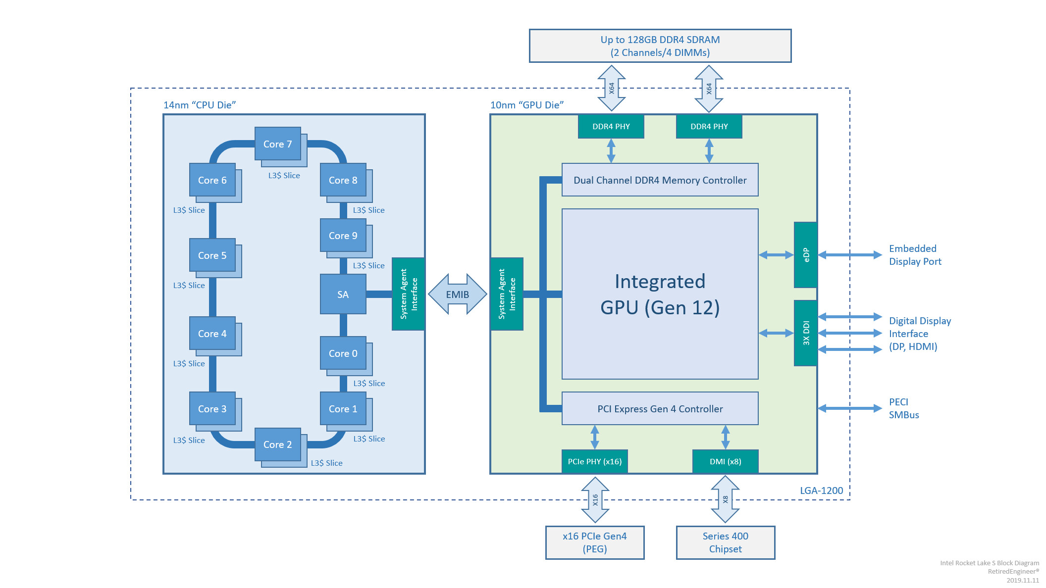
Apparently, "Rocket Lake-S" is a multi-chip module of a 14 nm die that holds the CPU cores; and 10 nm die that holds the uncore components. AMD "Matisse" and "Vermeer" too have such a division of labor, but the CPU cores are located on dies with a more advanced silicon fabrication process (7 nm), than the die with the uncore components (12 nm).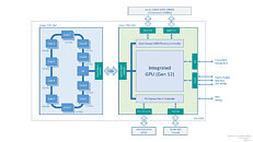 The 14 nm CPU die on "Rocket Lake-S" holds "Willow Cove" CPU cores that are purported to introduce significant IPC gains over "Skylake." In this die, there are CPU cores and a reduced-functionality system agent, which are bound together by a Ring-bus interconnect. This system agent talks to its counterpart on the uncore die (aka "GPU die"), over EMIB interconnect.
The 10 nm GPU die (aka uncore die) features the processor's Gen12 Xe iGPU with up to 96 execution units, a dual-channel DDR4 memory controller, and a PCI-Express 4.0 root-complex, besides other minor components related to the iGPU, such as its display- and media engines.
Unlike every past Intel mainstream desktop generation since "Lynnfield," the "Rocket Lake-S" MCM puts out a total of 24 PCI-Express lanes. 16 of these are assigned as PEG (PCI-Express Graphics, or the main PCI-Express x16 slot on the platform); and 8 lanes are assigned as chipset bus. In past microarchitectures, including "Comet Lake-S," the processor only put out 20 lanes, 16 of which are toward PEG, and 4 toward the chipset-bus (DMI).
This won't be the first time that Intel took the MCM approach in its mainstream desktop processors. The first generation "Clarkdale" desktop processor in the LGA1156 package was an MCM of a 32 nm CPU die, and a 45 nm uncore die (which contained the iGPU).
Why Intel chose to give the iGPU, rather than the CPU cores, the advantage of the more advanced silicon fabrication process is a mystery that will only be solved after launch. Perhaps it's simply not possible to build a Gen12 iGPU on 14 nm, while the efficiency of "Willow Cove" CPU cores, originally designed for 10 nm+, can survive a back-port to 14 nm better. "Willow Cove" cores make their debut with the "Tiger Lake-U" mobile processors.
Source:
Chiakokhua (Twitter)
Apparently, "Rocket Lake-S" is a multi-chip module of a 14 nm die that holds the CPU cores; and 10 nm die that holds the uncore components. AMD "Matisse" and "Vermeer" too have such a division of labor, but the CPU cores are located on dies with a more advanced silicon fabrication process (7 nm), than the die with the uncore components (12 nm).
The 10 nm GPU die (aka uncore die) features the processor's Gen12 Xe iGPU with up to 96 execution units, a dual-channel DDR4 memory controller, and a PCI-Express 4.0 root-complex, besides other minor components related to the iGPU, such as its display- and media engines.
Unlike every past Intel mainstream desktop generation since "Lynnfield," the "Rocket Lake-S" MCM puts out a total of 24 PCI-Express lanes. 16 of these are assigned as PEG (PCI-Express Graphics, or the main PCI-Express x16 slot on the platform); and 8 lanes are assigned as chipset bus. In past microarchitectures, including "Comet Lake-S," the processor only put out 20 lanes, 16 of which are toward PEG, and 4 toward the chipset-bus (DMI).
This won't be the first time that Intel took the MCM approach in its mainstream desktop processors. The first generation "Clarkdale" desktop processor in the LGA1156 package was an MCM of a 32 nm CPU die, and a 45 nm uncore die (which contained the iGPU).
Why Intel chose to give the iGPU, rather than the CPU cores, the advantage of the more advanced silicon fabrication process is a mystery that will only be solved after launch. Perhaps it's simply not possible to build a Gen12 iGPU on 14 nm, while the efficiency of "Willow Cove" CPU cores, originally designed for 10 nm+, can survive a back-port to 14 nm better. "Willow Cove" cores make their debut with the "Tiger Lake-U" mobile processors.
23 Comments on Intel "Rocket Lake-S" a Multi-Chip Module of 14nm Core and 10nm Uncore Dies?
Is that glue I'm smelling?!
10nm/+ is (currently) unable to attain as high clocks as 14nm+++++++.
Intel was caught with their pants down because they were reliant on small monolithic dies where they could fit four cores and a GPU while keeping costs low. That doesn't scale up well to meet the competition AMD is bringing, which is brilliant.
It's great to see Intel gluing chips together.
Edit: oh and Tiger Lake is supposed to have 1.5x the EU of Ice Lake for the GPU which will also be Gen12. How will that affect the size? Only Intel knows ;)
The CPU portion 4C 41mm2 is removed and then upscaled to 14 nm and 128mm2 8C.
So the CPU is bigger in the end, and the GPU part isn't very likely to have 96ALu like in TGL but 24 instead.
To which Malory responded :"It's your house."