Monday, April 13th 2015

AMD "Zen" A Monolithic Core Design
AMD's upcoming "Zen" architecture will see a major change in the way the company designs its CPU cores. It will be a departure from the "module" core design introduced with "Bulldozer," in which two cores with shared resources constitute the indivisible unit of a multi-core processor. A "Zen" core will have dedicated resources in a way things used to be before "Bulldozer," and only the last-level cache (L3 cache), will be shared between cores. "Zen" will also implement SMT, much in the same way as Intel processors do, with HyperThreading Technology.
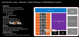
The first implementation of "Zen" will be an insanely powerful APU (on paper anyway), featuring 16 physical "Zen" CPU cores, 32 logical CPUs enabled with SMT, 512 KB dedicated L2 cache per core, and 32 MB of shared L3 cache. The CPU's ISA instruction set will see a spring-cleaning, with the removal of underused instruction-sets, and the introduction of new ones. Other features on this APU are equally surprising - a quad-channel DDR4 integrated memory controller, a separate HBM (high-bandwidth memory) controller dedicated to the integrated graphics, with up to 512 GB/s bandwidth, and an integrated graphics core featuring "Greenland-class" stream processors. Given that AMD is able to build 7-billion transistor GPUs on existing 28 nm processes, building an APU with these chops doesn't sound far-fetched. The company could still have to rely on a newer fab.
Source:
FudZilla
The first implementation of "Zen" will be an insanely powerful APU (on paper anyway), featuring 16 physical "Zen" CPU cores, 32 logical CPUs enabled with SMT, 512 KB dedicated L2 cache per core, and 32 MB of shared L3 cache. The CPU's ISA instruction set will see a spring-cleaning, with the removal of underused instruction-sets, and the introduction of new ones. Other features on this APU are equally surprising - a quad-channel DDR4 integrated memory controller, a separate HBM (high-bandwidth memory) controller dedicated to the integrated graphics, with up to 512 GB/s bandwidth, and an integrated graphics core featuring "Greenland-class" stream processors. Given that AMD is able to build 7-billion transistor GPUs on existing 28 nm processes, building an APU with these chops doesn't sound far-fetched. The company could still have to rely on a newer fab.

102 Comments on AMD "Zen" A Monolithic Core Design
Not sure what I really think beyond it sounds great on paper though. It could really be a huge step up from them and I am sure it will be lots better than the previous gen CPU's, however it will come down to how much on a clock to clock ratio as to whether these things are just good or fantastic.
Meanwhile, Zen is a new µArch – a completely new design.
So, it can't be, in any way, just one "beefy" updated Jaguar, i.e. Puma.
AMD should at least match Sandy Bridge's IPC this time, otherwise the same story will repeat... and please, don't call these "FX".
They also look like jaguar derivatives.
You want performance for your own selfish needs, which is fine, but don't pretend more performance will magically change the "story" without a strategic business plan.
AMD's Ad guys had everyone worked up into a frenzy with a lot of fantastic, dubious claims about its performance.
Then, It came out and everyone was underwhelmed and pissed off about it.
They took a huge PR hit then, and not long afterwards, they fired most of the Ad guys responsible.
I think that they learned from that and have toned down the rhetoric since then.
Me, I'm now cautious about new releases. I want to see reviews, and not just one of them either.
I want to read about other's experiences with brand new tech before I spend money getting into it.
I don't care if I'm the first one to have something anymore.
Zen ~sounds~ really good, but show me the reviews first.