Monday, March 14th 2016

AMD Unveils GPU Architecture Roadmap, "Polaris" to Skip HBM2 Memory?
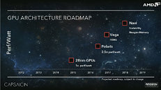
Alongside its big Radeon Pro Duo flagship graphics card launch, AMD unveiled its GPU architecture roadmap that looks as far into the future as early-2018. By then, AMD will have launched as many as three new GPU architectures. It begins with the launch of its 4th generation Graphics CoreNext architecture, codenamed "Polaris," in mid-2016. Built on the 14 nm FinFET process, "Polaris" is expected to offer a whopping 2.5x increase in performance-per-Watt for AMD, compared to its current GCN 1.2 architecture on 28 nm.
Hot on Polaris' heels, in early-2017, AMD plans to launch the "Vega" GPU architecture. While this appears to offer a 50% increase in performance-per-Watt over Polaris, its highlight is HBM2 memory. Does this mean that AMD plans to skip HBM2 on Polaris, and stick to GDDR5X? Could AMD be opting for a similar approach to NVIDIA, by launching its performance-segment GPU first as an enthusiast product, giving it a free run on the markets till early-2017, and then launching a Vega-based big-chip with HBM2 memory, taking over as the enthusiast-segment product? Some time in early-2018, AMD will launch the "Navi" architecture, which appears to offer a 2.5x performance-per-Watt lead over Polaris, taking advantage of an even newer memory standard.
Hot on Polaris' heels, in early-2017, AMD plans to launch the "Vega" GPU architecture. While this appears to offer a 50% increase in performance-per-Watt over Polaris, its highlight is HBM2 memory. Does this mean that AMD plans to skip HBM2 on Polaris, and stick to GDDR5X? Could AMD be opting for a similar approach to NVIDIA, by launching its performance-segment GPU first as an enthusiast product, giving it a free run on the markets till early-2017, and then launching a Vega-based big-chip with HBM2 memory, taking over as the enthusiast-segment product? Some time in early-2018, AMD will launch the "Navi" architecture, which appears to offer a 2.5x performance-per-Watt lead over Polaris, taking advantage of an even newer memory standard.

46 Comments on AMD Unveils GPU Architecture Roadmap, "Polaris" to Skip HBM2 Memory?
And you heard about the problems AMD had with Fiji??
And because you know you need some specialized test equipment for HBM??
Oh and if you just make one tiny mistake, you can flush a whole buch of working dice down the toilet...
The one thing I will give is that yes, AMD innovated again with HBM. But without it, Fiji would be really bad compared to Maxwell. Slightly higher power draw with HBM (about 10%) and the higher res performance would have not improved as it does. However, pioneering isn't always great for the present. Sometimes pioneers get overtaken by someone who implements things better. Given how much shouting (PR wise) AMD is doing right now, it's a little bit disconcerting this is bluster to me. Got a bad feeling Polaris won't be the Godly card we're all expecting.
If you had been paying attention, you would know that HBM is basically a well understood DDR technology whose only real innovation is the stacked die nature of the memory IC's. The difficulty lies not in its implementation but its manufacture and assembly - neither of which are the down to Nvidia/AMD. Hynix and Samsung manufacture the HBM, UMC and TSMC manufacture the interposer, and Amkor and ASE (and probably TSMC) assemble the GPU+HBM+Interposer package.
Here is a graphic representation of who is actually responsible for the technology implementation if you are still in a state of confusion.
Back to topic. For AMD, using HBM for at least two generation makes sense though. There is also no chance for a switch to GDDR5X now after spending that much resource on HBM. They just have to deal with the 4GB limit though.
Meanwhile, there is no way nVidia would be allowed to use HBM for free. Hence, they would make a move on GDDR5X when HBM2 is not available for mass production. Still GDDR5X is different from GDDR5. They still need time to implement it perfectly or face the disaster of Fermi with GDDR5 again.
AMD: We are actively promoting HBM and do not collect royalties Note that this also covers subsequent revisions to the standard such as JESD235A (HBM2).Not that different from what I've seen. A doubled prefetch is the biggest takeaway, and Micron have had GDDR5X in the wild for some time, and the GDDR5X emulation tools for memory controllers and physical layers has also been around for some time....
You can handsolder GDDR4 and 4 onto a PCB. Good luck with HBM...
The specs mean shit if you are unable to use it. And why the hell would you let nVidia just have HBM?!
Well, they can have it, but it does mean shit because they just can't put everything together!
I think you haven't thought about HBM at all and just say some shit without knowing anything!
With HBM you NEED this highly precise equipment and there aren't many companys out there able to put everything together. Bad luck for nVidia who let others develop the good stuff and come around when everything is done...
AMD and the development partners invested a great amount of money in this new technology and they should just give it to nVidia?! are you kidding?!
As said eariler, the spec means shit, because you have to put everything together, with GDDR4 and 5 you can do it by hand, with HBM that's impossible!
So they _NEED_ pretty damn expansive and precise equipment - something that wasn't around before, that's completely new and developed explicitely for HBM!
As for the Polaris chips:
AMD said there will be _TWO_ chips, one with HBM (the bigger one) and one without HBM...
Why the hell should there now be just one chip?!
Just because of some shitty roadmap?!
All you need is a decent hot air station and off you go...
Both companies have been saying for the last year that they will be using HBM in the future. This is nothing new.
Besides, it's non-sensical to complain about the lack of HBM2 in March, when HBM2 memory itself won't be available till September at the earliest.