Monday, November 6th 2017

Intel Announces "Coffee Lake" + AMD "Vega" Multi-chip Modules
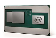
Rumors of the unthinkable silicon collaboration between Intel and AMD are true, as Intel announced its first multi-chip module (MCM), which combines a 14 nm Core "Coffee Lake-H" CPU die, with a specialized 14 nm GPU die by AMD, based on the "Vega" architecture. This GPU die has its own HBM2 memory stack over a 1024-bit wide memory bus. Unlike on the AMD "Vega 10" and "Fiji" MCMs, in which a silicon interposer is used to connect the GPU die to the memory stacks, Intel deployed the Embedded Multi-Die Interconnect Bridge (EMIB), a high-density substrate-level wiring. The CPU and GPU dies talk to each other over PCI-Express gen 3.0, wired through the package substrate.
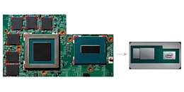
This multi-chip module, with a tiny Z-height, significantly reduces the board footprint of the CPU + discrete graphics implementation, when compared to having separate CPU and GPU packages with the GPU having discrete GDDR memory chips, and enables a new breed of ultra portable notebooks that pack a solid graphics muscle. The MCM should enable devices as thin as 11 mm. The specifications of the CPU and dGPU dies remain under the wraps. The first devices with these MCMs will launch by Q1 2018.A video presentation follows.
This multi-chip module, with a tiny Z-height, significantly reduces the board footprint of the CPU + discrete graphics implementation, when compared to having separate CPU and GPU packages with the GPU having discrete GDDR memory chips, and enables a new breed of ultra portable notebooks that pack a solid graphics muscle. The MCM should enable devices as thin as 11 mm. The specifications of the CPU and dGPU dies remain under the wraps. The first devices with these MCMs will launch by Q1 2018.A video presentation follows.


51 Comments on Intel Announces "Coffee Lake" + AMD "Vega" Multi-chip Modules