Friday, January 11th 2019

AMD Radeon VII Detailed Some More: Die-size, Secret-sauce, Ray-tracing, and More
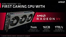
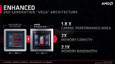
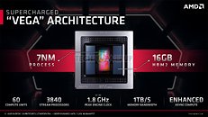
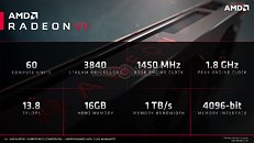
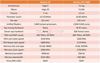
AMD pulled off a surprise at its CES 2019 keynote address, with the announcement of the Radeon VII client-segment graphics card targeted at gamers. We went hands-on with the card earlier this week. The company revealed a few more technical details of the card in its press-deck for the card. To begin with, the company talks about the immediate dividends of switching from 14 nm to 7 nm, with a reduction in die-size from 495 mm² on the "Vega 10" silicon to 331 mm² on the new "Vega 20" silicon. The company has reworked the die to feature a 4096-bit wide HBM2 memory interface, the "Vega 20" MCM now features four 32 Gbit HBM2 memory stacks, which make up the card's 16 GB of memory. The memory clock has been dialed up to 1000 MHz from 945 MHz on the RX Vega 64, which when coupled with the doubled bus-width, works out to a phenomenal 1 TB/s memory bandwidth.
We know from AMD's late-2018 announcement of the Radeon Instinct MI60 machine-learning accelerator based on the same silicon that "Vega 20" features a total of 64 NGCUs (next-generation compute units). To carve out the Radeon VII, AMD disabled 4 of these, resulting in an NGCU count of 60, which is halfway between the RX Vega 56 and RX Vega 64, resulting in a stream-processor count of 3,840. The reduced NGCU count could help AMD harvest the TSMC-built 7 nm GPU die better. AMD is attempting to make up the vast 44 percent performance gap between the RX Vega 64 and the GeForce RTX 2080 with a combination of factors.First, AMD appears to be maximizing the clock-speed headroom achieved from the switch to 7 nm. The Radeon VII can boost its engine clock all the way up to 1800 MHz, which may not seem significantly higher than the on-paper 1545 MHz boost frequency of the RX Vega 64, but the Radeon VII probably sustains its boost frequencies better. Second, the slide showing the competitive performance of Radeon VII against the RTX 2080 pins its highest performance gains over the NVIDIA rival in the "Vulkan" title "Strange Brigade," which is known to heavily leverage asynchronous-compute. AMD continues to have a technological upper-hand over NVIDIA in this area. AMD mentions "enhanced" asynchronous-compute for the Radeon VII, which means the company may have improved the ACEs (async-compute engines) on the "Vega 20" silicon, specialized hardware that schedule async-compute workloads among the NGCUs. With its given specs, the Radeon VII has a maximum FP32 throughput of 13.8 TFLOP/s
The third and most obvious area of improvement is memory. The "Vega 20" silicon is lavishly endowed with 16 GB of "high-bandwidth cache" memory, which thanks to the doubling in bus-width and increased memory clocks, results in 1 TB/s of memory bandwidth. Such high physical bandwidth could, in theory, allow AMD's designers to get rid of memory compression which probably frees up some of the GPU's number-crunching resources. The memory size also helps. AMD is once again throwing brute bandwidth to overcome any memory-management issues its architecture may have.The Radeon VII is being extensively marketed as a competitor to GeForce RTX 2080. NVIDIA holds a competitive edge with its hardware being DirectX Raytracing (DXR) ready, and even integrated specialized components called RT cores into its "Turing" GPUs. The "Vega 20" continues to lack such components, however AMD CEO Dr. Lisa Su confirmed at her post-keynote press round-table that the company is working on ray-tracing. "I think ray tracing is important technology; it's something that we're working on as well, from both a hardware/software standpoint."
Responding to a specific question by a reporter on whether AMD has ray-tracing technology, Dr. Su said: "I'm not going to get into a tit for tat, that's just not my style. So I'll tell you that. What I will say is ray tracing is an important technology. It's one of the important technologies; there are lots of other important technologies and you will hear more about what we're doing with ray tracing. You know, we certainly have a lot going on, both hardware and software, as we bring up that entire ecosystem."
One way of reading between the lines would be - and this is speculation on our part - that AMD could working on retrofitting some of its GPUs powerful enough to handle raytracing with DXR support through a future driver update, as well as working on future generations of GPUs with hardware-acceleration for many of the tasks that are required to get hybrid rasterization work (adding real-time raytraced objects to rasterized 3D scenes). Just as real-time raytracing is technically possible on "Pascal" even if daunting on the hardware, with good enough work directed at getting a ray-tracing model to work on NGCUs leveraging async-compute, some semblance of GPU-accelerated real-time ray-tracing compatible with DXR could probably be achieved. This is not a part of the feature-set of Radeon VII at launch.
The Radeon VII will be available from 7th February, priced at $699, which is on-par with the SEP of the RTX 2080, despite the lack of real-time raytracing (at least at launch). AMD could shepherd its developer-relations on future titles being increasingly reliant on asynchronous compute, the "Vulkan" API, and other technologies its hardware is good at.
154 Comments on AMD Radeon VII Detailed Some More: Die-size, Secret-sauce, Ray-tracing, and More
In terms of raw ROPS read/write hardware capabilities,
VII's ROPS (64 ROPS at 1800Mhz connected to multi-MB L2 cache) is 2.7X of RX-580's ROPS (32 ROPS at 1340 Mhz connected to memory controllers)
VII's 1TB/s raw memory bandwidth is 4X of RX-580's 256GB/s raw memory bandwidth. Vega's DCC is slightly better than Polaris DCC.
At 1 Ghz, R9-290X's 1MB L2 cache has 1TB/s bandwidth, but this bandwidth is not connected to ROPS until Vega era IP. RX-480 and Fury X has 2 MB L2 cache and it's not connected to ROPS.
Xbox One X GPU has 2 MB L2 cache for TMU and 2MB render cache for ROPS (feature missing in Polaris IP).
For raster graphics, ROPS is the primary read/write units to expose the GPU TFLOPS into L2 cache and external memory bandwidth. AMD has been pushing for async compute which uses texture unit as read-write.
Nvidia's memory compression superiority with Pascal.
AMD needs to use quad stack HBM v2's 1 TB/s memory bandwidth to rival RTX 2080's effective memory bandwidth.