Thursday, January 10th 2019

AMD Radeon VII Detailed Some More: Die-size, Secret-sauce, Ray-tracing, and More
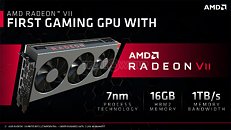
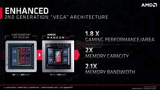
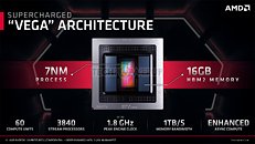
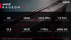
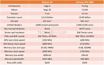
AMD pulled off a surprise at its CES 2019 keynote address, with the announcement of the Radeon VII client-segment graphics card targeted at gamers. We went hands-on with the card earlier this week. The company revealed a few more technical details of the card in its press-deck for the card. To begin with, the company talks about the immediate dividends of switching from 14 nm to 7 nm, with a reduction in die-size from 495 mm² on the "Vega 10" silicon to 331 mm² on the new "Vega 20" silicon. The company has reworked the die to feature a 4096-bit wide HBM2 memory interface, the "Vega 20" MCM now features four 32 Gbit HBM2 memory stacks, which make up the card's 16 GB of memory. The memory clock has been dialed up to 1000 MHz from 945 MHz on the RX Vega 64, which when coupled with the doubled bus-width, works out to a phenomenal 1 TB/s memory bandwidth.
We know from AMD's late-2018 announcement of the Radeon Instinct MI60 machine-learning accelerator based on the same silicon that "Vega 20" features a total of 64 NGCUs (next-generation compute units). To carve out the Radeon VII, AMD disabled 4 of these, resulting in an NGCU count of 60, which is halfway between the RX Vega 56 and RX Vega 64, resulting in a stream-processor count of 3,840. The reduced NGCU count could help AMD harvest the TSMC-built 7 nm GPU die better. AMD is attempting to make up the vast 44 percent performance gap between the RX Vega 64 and the GeForce RTX 2080 with a combination of factors.First, AMD appears to be maximizing the clock-speed headroom achieved from the switch to 7 nm. The Radeon VII can boost its engine clock all the way up to 1800 MHz, which may not seem significantly higher than the on-paper 1545 MHz boost frequency of the RX Vega 64, but the Radeon VII probably sustains its boost frequencies better. Second, the slide showing the competitive performance of Radeon VII against the RTX 2080 pins its highest performance gains over the NVIDIA rival in the "Vulkan" title "Strange Brigade," which is known to heavily leverage asynchronous-compute. AMD continues to have a technological upper-hand over NVIDIA in this area. AMD mentions "enhanced" asynchronous-compute for the Radeon VII, which means the company may have improved the ACEs (async-compute engines) on the "Vega 20" silicon, specialized hardware that schedule async-compute workloads among the NGCUs. With its given specs, the Radeon VII has a maximum FP32 throughput of 13.8 TFLOP/s
The third and most obvious area of improvement is memory. The "Vega 20" silicon is lavishly endowed with 16 GB of "high-bandwidth cache" memory, which thanks to the doubling in bus-width and increased memory clocks, results in 1 TB/s of memory bandwidth. Such high physical bandwidth could, in theory, allow AMD's designers to get rid of memory compression which probably frees up some of the GPU's number-crunching resources. The memory size also helps. AMD is once again throwing brute bandwidth to overcome any memory-management issues its architecture may have.The Radeon VII is being extensively marketed as a competitor to GeForce RTX 2080. NVIDIA holds a competitive edge with its hardware being DirectX Raytracing (DXR) ready, and even integrated specialized components called RT cores into its "Turing" GPUs. The "Vega 20" continues to lack such components, however AMD CEO Dr. Lisa Su confirmed at her post-keynote press round-table that the company is working on ray-tracing. "I think ray tracing is important technology; it's something that we're working on as well, from both a hardware/software standpoint."
Responding to a specific question by a reporter on whether AMD has ray-tracing technology, Dr. Su said: "I'm not going to get into a tit for tat, that's just not my style. So I'll tell you that. What I will say is ray tracing is an important technology. It's one of the important technologies; there are lots of other important technologies and you will hear more about what we're doing with ray tracing. You know, we certainly have a lot going on, both hardware and software, as we bring up that entire ecosystem."
One way of reading between the lines would be - and this is speculation on our part - that AMD could working on retrofitting some of its GPUs powerful enough to handle raytracing with DXR support through a future driver update, as well as working on future generations of GPUs with hardware-acceleration for many of the tasks that are required to get hybrid rasterization work (adding real-time raytraced objects to rasterized 3D scenes). Just as real-time raytracing is technically possible on "Pascal" even if daunting on the hardware, with good enough work directed at getting a ray-tracing model to work on NGCUs leveraging async-compute, some semblance of GPU-accelerated real-time ray-tracing compatible with DXR could probably be achieved. This is not a part of the feature-set of Radeon VII at launch.
The Radeon VII will be available from 7th February, priced at $699, which is on-par with the SEP of the RTX 2080, despite the lack of real-time raytracing (at least at launch). AMD could shepherd its developer-relations on future titles being increasingly reliant on asynchronous compute, the "Vulkan" API, and other technologies its hardware is good at.
154 Comments on AMD Radeon VII Detailed Some More: Die-size, Secret-sauce, Ray-tracing, and More
This time around Radeon VII is the one with less innovation. Even less so if we look at gaming. Not sure if 1:2 FP64 and wider memory bus count as innovation here.
All that is architecturally speaking. 7nm is a quality on its own :)
lel man volta 3000$ xDit not :x but I wish it was: if games used high precision computations it could give better graphics but I think the cards would burn becouse high power will used and temperature...
you don't think graphics is lower when used 16 bit float insted of 32 bit ?
I meen in sound this the true, more bit/sample give more quality.
there is also floated textures, I don't realy understand whay it don't need, it a trade ? more speed over more quality ? or more accuracy don't give more quality at all ?
I know GIMP have float point mode operation, and on the right monitor it realy look good...
4MB L2 cache
12 TFLOPS at 1340 Mhz,
64 ROPS at 1340 Mhz, bottlenecked problem. Polaris ROPS are not connected to L2 cache, hence highly dependant on external memory performance when compared to Vega 64 ROPS.
8 raster engines at 1340 Mhz, equivalent to six raster engines at 1800Mhz
512 GB/s memory bandwidth.
Still has problems with 64 ROPS at low clock speed.
Ideally, Vega M GH 2X wide would have
48 CU at 1536 Mhz would yield 9.4 TFLOPS
8 raster engines with 8 Shader Engines at 1536 Mhz
128 ROPS at 1536 MhzDLSS is just pixel reconstruction with multiple samples from previous frames which sounds like PS4 Pro's pixel reconstruction process.
www.pcgamer.com/nvidia-turing-architecture-deep-dive/
[INDENT]On previous architectures, the FP cores would have to stop their work while the GPU handled INT instructions, but now the scheduler can dispatch both to independent paths. This provides a theoretical immediate performance improvement of 35 percent per core.[/INDENT]
devblogs.nvidia.com/nvidia-turing-architecture-in-depth/
[INDENT]Turing introduces a new processor architecture, the Turing SM, that delivers a dramatic boost in shading efficiency, achieving 50% improvement in delivered performance per CUDA Core compared to the Pascal generation. These improvements are enabled by two key architectural changes. First, the Turing SM adds a new independent integer datapath that can execute instructions concurrently with the floating-point math datapath. In previous generations, executing these instructions would have blocked floating-point instructions from issuing.[/INDENT]
[INDENT][/INDENT]
[INDENT][/INDENT]
devblogs.nvidia.com/nvidia-turing-architecture-in-depth/
[INDENT]Turing Tensor Cores add new INT8 and INT4 precision modes for inferencing workloads that can tolerate quantization and don’t require FP16 precision. Turing Tensor Cores bring new deep learning- based AI capabilities to GeForce gaming PCs and Quadro-based workstations for the first time. A new technique called Deep Learning Super Sampling (DLSS) is powered by Tensor Cores. DLSS leverages a deep neural network to extract multidimensional features of the rendered scene and intelligently combine details from multiple frames to construct a high-quality final image[/INDENT]
VII supports INT8 and INT4 for deep learning- based AI capabilities.
Refer to Microsoft's DirectML. Read www.highperformancegraphics.org/wp-content/uploads/2018/Hot3D/HPG2018_DirectML.pdf
www.techspot.com/review/1762-just-cause-4-benchmarks/
RTX 2080 has 4 MB L2 cache while GTX 1080 Ti has ~3 MB L2 cache. This is important for tile cache rendering.
2. Wrong, Without memory bandwidth increase, Vega 56 at 1710 Mhz with faster ROPS and raster engines beating Strix Vega 64 at 1590 Mhz shows VII's direction with 1800 Mhz with memory bandwidth increase.
3. NCU itself doesn't compete the graphics pipeline.
4. RX-580 has delta color compression, 2 MB L2 cache for TMU and geometry (not connected to ROPS), higher clock speed for geometry/quad rastizer units and 8 GB VRAM selection.
R9-290X/R9-390X wasn't updated with Polaris IP upgrades. R9-390X has 8 GB VRAM.
Only Xbox One X's 44 CU GPU has the updates. NAVI 12 has 40 CU with unknown ROPS count, 256 bit GDDR6 and clock speed comparable to VII
You selected NVIDIA gameworks tile with geometry bias, NV GPUs has higher clock speed for geometry and raster engines.
RTX 2080 has six GPC with six raster engines, 4MB L2 cache and 64 ROPS with up to 1900 Mhz stealth overclock. Higher L2 cache storage = lower latency, less external memory hit rates.
GTX 1080 Ti has six GPC with six raster engines, 3MB L2 cache and 88 ROPS with up to 1800 Mhz stealth overclock.
R9-390X's 5.9 TFLOPS beats RX-480's 5.83 TFLOPS
R9-390 Pro's 5.1 TFLOPS beats RX-480's 5.83 TFLOPS
2. So what? Just Cause 4 is a Gameworks title. Avalanche Studios knows ROPS bound workaround with TMUs
Without Gameworks,
By 2160p AMD cards will drop off far faster than Nvidia counterparts.
Vega 64 has inferior delta color compression when compared NVIDIA's version which is remedied by VII's higher 1TB/s memory bandwidth.
Edit: Apparently Radeon VII can use DirectML which in practice can replace DLSS:
www.overclock3d.net/news/gpu_displays/amd_s_radeon_vii_supports_directml_-_an_alternative_to_dlss/1
That may imply that Vega 20 has tensor cores.
You cannot compare L2 client ROPs memory controller's overclock range with discrete ROPs memory controller. The memory controller of L2-ROPs only dispatches batched transactions, it has much less traffic since you need to hit maximum memory transfer rate to hit its 'actual' clock. ROPs are at a different frequency than the memory controller.
VII's 1.8Ghz scaling would be about 1.8 TB/s L2 cache bandwidth. Vega has compressed texture I/O from external memory.
Don't make me run CUDA app L2 cache benchmark on my GTX 1080 Ti and GTX 980 Ti.On older DX12 hardware, all lesser datatypes are either emulated into 32bit datatype or run at the same rate as 32bit datatype while newer hardware has higher performance benefits.
DirectML is important for uniformed API access to rapid pack math features in newer hardware while offer software compatibility with older hardware. DirectML benefits the next Xbox One hardware release.
Polaris GPU already pack math feature but it's usage doesn't increase TFLOPS rate and reduces the available stream processors for 32bit datatypes while Vega fixes this Polaris issue.R9-290X at 1Ghz has 1TB/s L2 bandwidth while GTX 980 Ti has about 600 GB/s L2 bandwidth (via CUDA app, disables DCC). R9-290X's ROPS are not connected to L2 cache while GTX 980 Ti's ROPS are connected to L2 cache (for tile cache render loop).
VII's 1800Mhz scale from R9-290X's 1Ghz design reaches to 1.8 TB/s L2 cache bandwidth.
Vega 56/64 has 4MB L2 cache for TMU and ROPS.1. Vega 56/64 has 4MB L2 cache. www.tomshardware.com/news/visiontek-radeon-rx-vega-64-graphics-card,35280.html
2. Not complete. Geometry/Raster Engines are another problem for AMD GPUs when NVIDIA GPU counterparts has higher clockspeed. Vega 56 at 1710Mhz with 12 TFLOPS beating Strix Vega 64 at 1590Mhz with 13 TFLOPS shows higher clockspeed improves Geometry/Raster Engines/ROPS/L2 cache despite Vega 56's lower TFLOPS.
3. Don't deny Gameworks issues. Hint: Geometry and related rasterization conversion process, and NVIDIA GPU counterparts has higher clockspeed that benefits classic GPU hardware. I advocate for AMD to reduce CU count (reduce power consumption) and trade for higher clock speed e.g. Vega 48 with 1900Mhz to 2Ghz range.
NVIDIA Maxwell/Pascal/Turing GPUs doesn't have PowerVR's "deferred tile render" but it has immediate mode tile cache render.
For my GTX 1080 Ti and 980 Ti GPUs, I can increase L2 cache bandwidth with an overclock.
Vega 56 at higher clock speed still has performance increase without increasing memory bandwidth and Vega ROPS has multi-MB L2 cache connection like Maxwell/Pascal's ROPS designs.
VII rivalling the fastest Turing GPU with 64 ROPS would be RTX 2080.
Battlefield series games are well known for software tiled compute render techniques which maximises older AMD GCNs with L2 cache connections with TMUs.
For Vega architecture from radeon.com/_downloads/vega-whitepaper-11.6.17.pdf
From AMD's white paper
Vega uses a relatively small number of tiles, and it operates on primitive batches of limited size compared with those used in previous tile-based rendering architectures. This setup keeps the costs associated with clipping and sorting manageable for complex scenes while delivering most of the performance and efficiency benefits.
AMD Vega Whitepaper:
[INDENT]The Draw-Stream Binning Rasterizer (DSBR) is an important innovation to highlight. It has been designed to reduce unnecessary processing and data transfer on the GPU, which helps both to boost performance and to reduce power consumption. The idea was to combine the benefits of a technique already widely used in handheld graphics products (tiled rendering) with the benefits of immediate-mode rendering used high-performance PC graphics.[/INDENT]
[INDENT]Pixel shading can also be deferred until an entire batch has been processed, so that only visible foreground pixels need to be shaded. This deferred step can be disabled selectively for batches that contain polygons with transparency. Deferred shading reduces unnecessary work by reducing overdraw (i.e., cases where pixel shaders are executed multiple times when di erent polygons overlap a single screen pixel).[/INDENT]
PowerVR's deferred tile render is patent heavy.