Thursday, January 10th 2019

AMD Radeon VII Detailed Some More: Die-size, Secret-sauce, Ray-tracing, and More
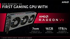
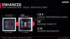
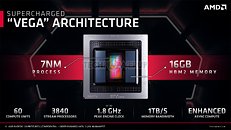
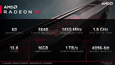
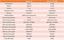
AMD pulled off a surprise at its CES 2019 keynote address, with the announcement of the Radeon VII client-segment graphics card targeted at gamers. We went hands-on with the card earlier this week. The company revealed a few more technical details of the card in its press-deck for the card. To begin with, the company talks about the immediate dividends of switching from 14 nm to 7 nm, with a reduction in die-size from 495 mm² on the "Vega 10" silicon to 331 mm² on the new "Vega 20" silicon. The company has reworked the die to feature a 4096-bit wide HBM2 memory interface, the "Vega 20" MCM now features four 32 Gbit HBM2 memory stacks, which make up the card's 16 GB of memory. The memory clock has been dialed up to 1000 MHz from 945 MHz on the RX Vega 64, which when coupled with the doubled bus-width, works out to a phenomenal 1 TB/s memory bandwidth.
We know from AMD's late-2018 announcement of the Radeon Instinct MI60 machine-learning accelerator based on the same silicon that "Vega 20" features a total of 64 NGCUs (next-generation compute units). To carve out the Radeon VII, AMD disabled 4 of these, resulting in an NGCU count of 60, which is halfway between the RX Vega 56 and RX Vega 64, resulting in a stream-processor count of 3,840. The reduced NGCU count could help AMD harvest the TSMC-built 7 nm GPU die better. AMD is attempting to make up the vast 44 percent performance gap between the RX Vega 64 and the GeForce RTX 2080 with a combination of factors.First, AMD appears to be maximizing the clock-speed headroom achieved from the switch to 7 nm. The Radeon VII can boost its engine clock all the way up to 1800 MHz, which may not seem significantly higher than the on-paper 1545 MHz boost frequency of the RX Vega 64, but the Radeon VII probably sustains its boost frequencies better. Second, the slide showing the competitive performance of Radeon VII against the RTX 2080 pins its highest performance gains over the NVIDIA rival in the "Vulkan" title "Strange Brigade," which is known to heavily leverage asynchronous-compute. AMD continues to have a technological upper-hand over NVIDIA in this area. AMD mentions "enhanced" asynchronous-compute for the Radeon VII, which means the company may have improved the ACEs (async-compute engines) on the "Vega 20" silicon, specialized hardware that schedule async-compute workloads among the NGCUs. With its given specs, the Radeon VII has a maximum FP32 throughput of 13.8 TFLOP/s
The third and most obvious area of improvement is memory. The "Vega 20" silicon is lavishly endowed with 16 GB of "high-bandwidth cache" memory, which thanks to the doubling in bus-width and increased memory clocks, results in 1 TB/s of memory bandwidth. Such high physical bandwidth could, in theory, allow AMD's designers to get rid of memory compression which probably frees up some of the GPU's number-crunching resources. The memory size also helps. AMD is once again throwing brute bandwidth to overcome any memory-management issues its architecture may have.The Radeon VII is being extensively marketed as a competitor to GeForce RTX 2080. NVIDIA holds a competitive edge with its hardware being DirectX Raytracing (DXR) ready, and even integrated specialized components called RT cores into its "Turing" GPUs. The "Vega 20" continues to lack such components, however AMD CEO Dr. Lisa Su confirmed at her post-keynote press round-table that the company is working on ray-tracing. "I think ray tracing is important technology; it's something that we're working on as well, from both a hardware/software standpoint."
Responding to a specific question by a reporter on whether AMD has ray-tracing technology, Dr. Su said: "I'm not going to get into a tit for tat, that's just not my style. So I'll tell you that. What I will say is ray tracing is an important technology. It's one of the important technologies; there are lots of other important technologies and you will hear more about what we're doing with ray tracing. You know, we certainly have a lot going on, both hardware and software, as we bring up that entire ecosystem."
One way of reading between the lines would be - and this is speculation on our part - that AMD could working on retrofitting some of its GPUs powerful enough to handle raytracing with DXR support through a future driver update, as well as working on future generations of GPUs with hardware-acceleration for many of the tasks that are required to get hybrid rasterization work (adding real-time raytraced objects to rasterized 3D scenes). Just as real-time raytracing is technically possible on "Pascal" even if daunting on the hardware, with good enough work directed at getting a ray-tracing model to work on NGCUs leveraging async-compute, some semblance of GPU-accelerated real-time ray-tracing compatible with DXR could probably be achieved. This is not a part of the feature-set of Radeon VII at launch.
The Radeon VII will be available from 7th February, priced at $699, which is on-par with the SEP of the RTX 2080, despite the lack of real-time raytracing (at least at launch). AMD could shepherd its developer-relations on future titles being increasingly reliant on asynchronous compute, the "Vulkan" API, and other technologies its hardware is good at.
154 Comments on AMD Radeon VII Detailed Some More: Die-size, Secret-sauce, Ray-tracing, and More
Actually, I would prefer no developer relationships with either company because they are only good for one 'color'. Clearly, one of us needs a brain...
- Assetto Corsa Competizione
- Atomic Heart
- Battlefield V
- Control
- Enlisted
- Justice
- JX3
- MechWarrior 5: Mercenaries
- Metro Exodus
- ProjectDH
- Shadow of the Tomb Raider
As for DLSS, the list is longer:- Ark: Survival Evolved
- Anthem
- Atomic Heart
- Battlefield V
- Dauntless
- Final Fantasy 15
- Fractured Lands
- Hitman 2
- Islands of Nyne
- Justice
- JX3
- Mechwarrior 5: Mercenaries
- PlayerUnknown’s Battlegrounds
- Remnant: From the Ashes
- Serious Sam 4: Planet Badass
- Shadow of the Tomb Raider
- The Forge Arena
- We Happy Few
- Darksiders III
- Deliver Us The Moon: Fortuna
- Fear the Wolves
- Hellblade: Senua’s Sacrifice
- KINETIK
- Outpost Zero
- Overkill’s The Walking Dead
- SCUM
- Stormdivers
Again, the Radeon VII price is just too high. You'll notice I never criticize the product - it uses great memory and plenty of it. I like that feature. What I don't like is the high price and missing features. At a proper market price of 499-549 it is a winner. To end with a tip, users appear more credible if you post your comments without profanity and with support for facts.Data sources: www.digitaltrends.com/computing/games-support-nvidia-ray-tracing/ , www.kitguru.net/components/graphic-cards/matthew-wilson/here-are-the-first-games-set-to-support-nvidias-ray-tracing-and-dlss-rtx-features/
It has nothing to do with ROPs, having 64 ROPs is completely fine at up to 3840*2160p and won't cause any bottleneck.
Do you really think AMD is dumb enough to make GPUs that are bottlenecked by such a relatively simple thing?
Keep the discussions civil and on topic.
Thank You
GCNs problem is that the drivers (read: CPU) do more work than Maxwell+ do. This is why Vega and Fiji do not so great at low resolutions but well at high resolutions (CPU matters less). Vulkan and Direct3D 12 perform much better on GCN than Direct3D 11 because it naturally removes a lot of the underlying CPU burden.
I suspect Navi will take lessons learned from Xbox One and PlayStation 4 to produce hardware that needs minimal driver interference.
That doesn't mean you can't find an edge-case where more ROPs don't help, as with anything else, but that's beside the point.Well, it's true that Direct3D 12 and Vulkan can offload a lot of the management done by the drivers, but not the truly low-level allocation and resource management, which happens inside the GPU, and this is where GCN struggles.
Just like intel's advantage over AMD in gaming, my guess is that it has something to do with way lesser cache latencies on Nvidia GPUs.
Of course this isn't the full story.
Shadow of the Tomb Raider patch (shadows) and Metro Exodus (AO) should be a lot more interesting RTRT use cases once they show up.
It's not just about the final frame, because they aren't drawing the same uniform color 55 thousand times per second.
Every texel that needs to be placed somewhere on a scene also needs to be accessed. The ratio of texels read to pixels written might vary widely, but considering that modern games have millions of triangles on the screen, that's a whole lot of textures that need to be read and their data calculated in order to obtain the final pixel.
Obviously there's CU caching involved as well but the ratio is still huge.
Let's assume some numbers: If Texel to Pixel ratio is 20:1, and due to overdrawing more pixels are written than actually seen the display ratio is "only" 5:1 (might be much higher in complex scenes with a lot of translucency, edge anti-aliasing and more), that is already an 100:1 vs your number.
55 thousand fps is now just 550.
Add multi-sampling (4X) and now back to a more realistic 550 : 4 = 137 fps, which seems to be what these cards can do...
Just compare GTX 1080, RTX 2060 vs. Vega 64, three GPUs which perform similarly. While GTX 1080 had 102.8 - 110.9 GP/s, RTX 2060 reduced it to 65.52-80.54 GP/s (less than Vega 64's 79.8 - 98.9 GP/s), and still managed to maintain performance, even at 4K.
The issue with GCN is not the raw throughput of the various resources, it's the management of those resources.
For absolute performance, lowering time to completion in all graphics pipeline stages should be a priority. Your argument doesn't lead to lowest latency operation.
Where did you obtain Vega ROPS unit has 4 color pixels per clock? Each RB unit has four color ROPS and 16 z-ROPS. For 64 ROPS, that's 16 RB units x 4 color ROPS = 64 color ROPS, hence it's 64 color pixels per clock.
IF AMD is pushing for compute/256 TMUs read-write path, why not increase ROPS count to match TMU read-write performance?RTX 2060 (30 SM) has 48 ROPS at 1900 Mhz stealth overclock. Full TU106 (36 SM) has 4 MB L2 cache. Full GP104 has 2MB L2 cache. This is important for NVIDIA's immediate mode tile cache render loop and improves to lower latency which improves reduces time to completion timings.
We see the same thing with GTX 970, which has higher performance per clock than it's big brother GTX 980. Why? Because it struck a sweetspot in various resources.
Refer to Avalanche Studios lecture on TMU read-write workaround on ROPS bound situations.For AMD GCN, register files are with CU level. Each CU has it's own warp scheduling.
GTX 970 has 56 ROPS with less L2 cache.
GTX 980 has 64 ROPS
Vega 56 has full 64 ROPS and full 4MB L2 cache like Vega 64. VII's 60 CU still has full L2 cache and 64 ROPS access like MI60. Faster clock speed improves L2 cache and 64 ROPS i.e. lessen the time to completion.
Vega 56 running Vega 64 BIOS is 2% slower than Vega 64. That likely has less to do ROPs and more to do with underutilization of shaders as I previous said. Vega, and Fiji before it, were designed for server farms running compute loads. They were never ideal for gaming. Polaris, on the other hand, is biased towards gaming. It has 32 ROPs to 36 CUs (8:9 compared to Vega 64 1:1 or Vega 56 8:7) . Again, if ROPs were really the bottleneck, AMD would have put more ROPs on it but they didn't.
Vega and Fiji do exceptionally well in async games like Ashes of the Singularity because all of those shaders aren't so underutilized.
Again, read Avalanche Studios lecture on TMU read-write workaround on ROPS bound situations.
Btw: Vega M GH has 24 CU with 64 ROPS ratio.
For current Vega 64 type GPU, it's better to trade less CU count which reduce power consumption for higher clock speed which has higher ROPS/L2 cache/rasterization performance. Vega 56 at 1710 Mhz with 12 TFLOPS beating Strix Vega 64 OC at 1590Mhz with 13 TFLOPS.
Rasterization = floating point geometry to pixel integer mass conversion hardware.
Note the four Rasterzier hardware units, AMD increased this hardware during R9-290X's introduction before "Mr TFLOPS" joined AMD in 2013.
At higher clock speed, classic GPU hardware such as Rasterzier, Render Back End(ROPS) and L2 cache has higher performance i.e. lower time to completion.
At the same clock speed and L2 cache size, 88 ROPS has 88 pixels per clock has lower time completion when compared to 64 ROPS with 64 pixels per clock. AMD knows ROPS bound problem hence compute shader's read-write path workaround marketing push and VII's 1800Mhz clock speed with lower CU count.
NVIDIA's GPU designs has higher clock speeds to speed up classic GPU hardware.
Cryptocurrency uses TMU read-write path instead of ROPS read-write path.
AMD could have configured a GPU with 48 CU, 64 ROPS and 1900 Mhz
RX-580... AMD hasn't mastered 64 ROPS over 256 bit bus design, hence RX-580 is stuck at 32 ROPS with 256 bit bus. R9-290X has 64 ROPS with 512 bit bus which is 2X scale over R9-380X/RX-580's design.
How do things of that kind work, do authors of these texts simply root for nVidia, do they come from Huang's headquarters, are they somehow censored by NV's PR team?
Just curious.