News Posts matching #28 nm

Return to Keyword Browsing

TSMC Witnesses 28 nm Process Demand Soar

Recently, the technology trade war between the US and China has been very challenging for Chinese semiconductor manufacturers. With a new regulation to prevent the use of US technology on foreign lands, the US administration has managed to prevent many companies from manufacturing the latest processes, and they have lost a part of their customer base. In awe of this craze, it seems like many silicon designers are storming to the competing foundries to get their designs taped out. According to the DigiTimes report, TSMC has seen a massive spike in demand for its 28 nm semiconductor node. The surge is going to reach a peak of almost 100% in the fourth quarter this year. The growth is mainly being driven by Chinese customers who are switching their manufacturing facilities. The report indicated that Qualcomm, as well, is a big part of the growth besides the remaining companies.

Zhaoxin to Design Discrete GPUs

Zhaoxin, the Chinese chip-maker famous for Kaixian line of x86 processors, and a major beneficiary of the Chinese government's ambitious "3-5-2 plan" of public investment toward the country's computer hardware independence by the mid-2020s, unveiled plans to design its first discrete GPUs that could double up as scalar-compute and AI processors. The company's baby step is a tiny 70-Watt dGPU that will be fabricated on TSMC's 28 nm silicon fabrication process that will likely serve as a tech demonstrator and development platform for ISVs. The dGPU is largely expected to derive from VIA's S3 Graphics IP as VIA has collaborated with Zhaoxin as an iGPU provider for its Kaixian line of x86 SoCs.

Lattice Semiconductor Announces Certus-NX General Purpose FPGA

Lattice Semiconductor Corporation, the low power programmable leader, today launched the new Lattice Certus -NX family of FPGAs. The devices lead the general-purpose FPGA market in I/O density, delivering up to twice the I/O density per mm2 in comparison to similar competing FPGAs, and provide best-in-class power savings, small size, reliability, instant-on performance, and support fast PCI Express (PCIe) and Gigabit Ethernet interfaces to enable data co-processing, signal bridging, and system control. Certus-NX FPGAs target a range of applications, from data processing in automated industrial equipment to system management in communications infrastructure. The Certus-NX devices are the second family of FPGAs developed on the Lattice Nexus platform, the industry's first low power FPGA platform using 28 nm FD-SOI process technology. With the launch of Certus-NX, Lattice marks the release of the second device family developed under Lattice's new product development strategy in just six months.

"Certus-NX delivers unique and innovative capabilities that set it apart," said Linley Gwennap, Principal Analyst at The Linley Group. "Compared to competing FPGAs of similar gate counts, Lattice offers a much smaller package, greater I/O density, and lower power."
Everspin Technologies and GLOBALFOUNDRIES Extend MRAM Joint Development Agreement to 12nm

Everspin Technologies, Inc., the world's leading developer and manufacturer of Magnetoresistive RAM (MRAM), today announced an amendment of its Spin-transfer Torque (STT-MRAM) joint development agreement (JDA) with GLOBALFOUNDRIES (GF ), the world's leading specialty foundry. Everspin and GF have been partners on 40 nm, 28 nm, and 22 nm STT-MRAM development and manufacturing processes and have now updated their agreement to set the terms for a future project on an advanced 12 nm FinFET MRAM solution. Everspin is in production of discrete STT-MRAM solutions on 40 and 28 nm, including its award winning 1 Gb DDR4 device. GF recently announced it has achieved initial production of embedded MRAM (eMRAM) on its 22FDX platform.

CEA-Leti Makes a 96 core CPU from Six Chiplets

Chiplet design of processors is getting more popular due to many improvements and opportunities it offers. Some of the benefits include lower costs as the dies are smaller compared to one monolithic design, while you are theoretically able to stitch as much of the chiplets together as possible. During the ISSCC 2020 conference, CEA-Leti, a French research institute, created a 96 core CPU made from six 3D stacked 16 core chiplets. The chip is created as a demonstration of what this modular approach offers and what are the capabilities of the chiplet-based CPU design.

The chiplets are manufactured on the 28 nm FD-SOI manufacturing process from STMicroelectronics, while the active interposer die below them that is connecting everything is made using the 65 nm process. Each one of the six dies is housing 16 cores based on MIPS Instruction Set Architecture core. Each chiplet is split into four 4-core clusters that make up for a total of 16 cores per chiplet. When it comes to the core itself, it is a scalar MIPS32v1 core equipped with 16 KiB of L1 instruction and an L1 data cache. For L2 cache, there is 256 KiB per cluster, while the L3 cache is split into four 1 MiB tiles for the whole cluster. The chiplets are stacked on top of an active interposer which connects the chiplets and provides external I/O support.

Toshiba Develops New Bridge Chip Using PAM 4 to Boost SSD Speed and Capacity

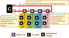
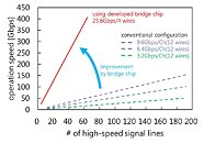
Toshiba Memory Corporation, the world leader in memory solutions, today announced the development of a bridge chip that realizes high-speed and large-capacity SSDs. Using developed bridge chips with a small occupied area and low-power consumption, the company has succeeded in connecting more flash memory chips with fewer high-speed signal lines than with the conventional method of no bridge chips. This result was announced in San Francisco on February 20, at the International Solid-State Circuits Conference 2019 (ISSCC 2019).

In SSDs, multiple flash memory chips are connected to a controller that manages their operation. As more flash memory chips are connected to a controller interface, operating speed degrades, so there are limits to the number of chips that can be connected. In order to increase capacity, it is necessary to increase the number of interfaces, but that results in an enormous number of high-speed signal lines connected to the controller, making it more difficult to implement the wiring on the SSD board.

TSMC Trade Secrets Stolen - Former Engineer Arrested In China

In the highly competitive, high-stakes scene of the business world - and particularly so in the silicon giants of the era - trade secrets, specifications, and protecting one's intellectual property that give the leg-up on competitors is key towards success. And while most companies work within the meanders of law (even if sometimes skirting it ever so lightly), some don't. And things like this happen: the steal (or purported steal, because no one has been convicted yet) of trade secrets by former employees is one of the most dreaded occurrences in the tech world - remember Zenimax and Carmack's "dovetailing"?

Chinese manufacturers are looking to enter the high-performance computing market with their own products, designs, and manufacturing capability. In this case, former TSMC engineer Hsu is being accused of stealing proprietary information and other materials related to the foundry's 28 nm process technology. The goal would be to pass them to China-based Shanghai Huali Microelectronics (HLMC), with which he accepted a job offer, according to the Hsinchu District Prosecutors Office. Digitimes reports that HLMC had been aggressively headhunting for talent to kick start its 28 nm manufacturing process, though if true, this sound like a little too aggressive of a headhunting.

Sapphire Unveils the Radeon R9 390 TOXIC Graphics Card

Sapphire unveiled its highest tuning air-cooled TOXIC variant for the Radeon R9 390. Targeted at the Greater China region (PRC, Hong Kong, Taiwan), this card features a swanky new VaporX vapor-chamber cooling solution, and the highest factory-overclock by the company for this chip. The core is clocked at 1120 MHz against reference clocks of 1000 MHz, and an untouched 6.00 GHz (GDDR5-effective) memory clock.

The cooling solution consists of a large vapor-chamber plate, from which a number of 8 mm-thick copper heat pipes convey heat to two aluminium fin stacks, which are ventilated by three 100 mm spinners. A chunky, ridged, aluminium base-plate covers nearly every other part of the PCB, cooling the VRM and memory chips. Based on the 28 nm "Grenada" silicon, the R9 390 features 2,560 stream processors, 160 TMUs, 64 ROPs, and a 512-bit wide GDDR5 memory interface, holding 8 GB of memory.
AMD Outs "Bristol Ridge" APU Performance Numbers

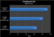
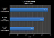
Although AMD's upcoming socket AM4 heralds new lines of processors and APUs based on the company's next-generation "Zen" CPU micro-architecture, some of the first APUs will continue to be based the current "Excavator" architecture. The "Bristol Ridge" is one such chip. It made its mobile debut as the 7th generation A-Series and FX-Series mobile APUs, and is en route to the desktop platform, in the AM4 package. What sets the AM4 package apart from the FM2+ package, and in turn "Bristol Ridge" from "Carrizo" is that the platform integrates even the southbridge (FCH) into the APU die. This could explain the 1,331-pin count of the AM4 socket.

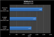
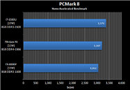
The "Bristol Ridge" silicon is likely built on the existing 28 nm process. That's not the only thing "current-gen" about this chip. Its CPU component consists of two "Excavator" modules that make up four CPU cores, with 4 MB total cache; and its integrated GPU will likely be based on the Graphics CoreNext 1.2 "Volcanic Islands" architecture, the same one which drives the "Tonga" and "Fiji" discrete GPUs. The integrated memory controller supports dual-channel DDR4 memory. In its performance benchmarks, an AM4 APU based on the "Bristol Ridge" silicon was pitted against older 6th generation APUs, in which it was found to be as much as 23 percent faster.

AMD Unveils GPU Architecture Roadmap, "Polaris" to Skip HBM2 Memory?

Alongside its big Radeon Pro Duo flagship graphics card launch, AMD unveiled its GPU architecture roadmap that looks as far into the future as early-2018. By then, AMD will have launched as many as three new GPU architectures. It begins with the launch of its 4th generation Graphics CoreNext architecture, codenamed "Polaris," in mid-2016. Built on the 14 nm FinFET process, "Polaris" is expected to offer a whopping 2.5x increase in performance-per-Watt for AMD, compared to its current GCN 1.2 architecture on 28 nm.

Hot on Polaris' heels, in early-2017, AMD plans to launch the "Vega" GPU architecture. While this appears to offer a 50% increase in performance-per-Watt over Polaris, its highlight is HBM2 memory. Does this mean that AMD plans to skip HBM2 on Polaris, and stick to GDDR5X? Could AMD be opting for a similar approach to NVIDIA, by launching its performance-segment GPU first as an enthusiast product, giving it a free run on the markets till early-2017, and then launching a Vega-based big-chip with HBM2 memory, taking over as the enthusiast-segment product? Some time in early-2018, AMD will launch the "Navi" architecture, which appears to offer a 2.5x performance-per-Watt lead over Polaris, taking advantage of an even newer memory standard.

AMD Unveils the Radeon Pro Duo Graphics Card

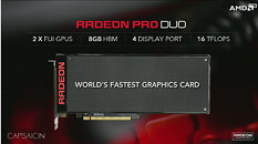
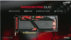
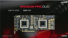
AMD unveiled its latest flagship graphics card, the Radeon Pro Duo. The card is designed for "creators who game, and gamers who create," as the tagline goes. It is a dual-GPU graphics card based on a pair of 28 nm "Fiji" chips, the same ones which drive the R9 Fury X and the R9 Nano. AMD is positioning this card in the gray-area between consumer graphics cards, and FirePro workstation products, as a new "workstation-class" product. Perhaps this allows the company to get away with things such as three 8-pin PCIe power connectors.

The Radeon Pro Duo features two "Fiji" GPUs in their maximum core configuration - 4,096 stream processors, 256 TMUs, and 64 ROPs, each; with 4 GB of HBM memory, each. The card hence packs a total of 8 GB HBM memory, and 16 TFLOP/s total single-precision floating-point performance. The card features a liquid-cooling solution designed by Cooler Master, with a thick 120 mm x 120 mm radiator that's similar to the one that ships with the R9 Fury X. The card's display output configuration is similar to the R9 Fury X, too, with three DisplayPort 1.2a and one HDMI 1.4a connectors. AMD is going ahead and claiming the title of "World's Fastest Graphics Card." The Radeon R9 Pro Duo is expected to be priced at US $1,499.

HIS Announces the Radeon R7 360 Green iCooler OC

HIS rolled out a new low-power Radeon R7 360 graphics card. The R7 360 Green iCooler OC, comes with TDP of 50W, compared to AMD's own specs that rate it at 100W. The card relies on the PCIe bus for entirely for its power, and uses high-grade VRM components that are more energy-efficient than the ones found on most R7 360 cards. That's not all, HIS is also throwing in a tiny OC - 1070 MHz core (vs. 1050 MHz reference). The card's 2 GB of GDDR5 memory over a 128-bit memory bus ticks at 6.00 GHz (GDDR5-effective). Based on the 28 nm "Tobago" silicon, the R7 360 packs 768 stream processors. In Europe, you can expect the HIS R7 360 Green iCooler OC to be priced at 99.90€ (including all taxes).

Marvell Industry-Leading SSD Controller Tech Expands the NVMe HMB Ecosystem

Marvell, a world leader in storage, cloud infrastructure, Internet of Things (IoT), connectivity and multimedia semiconductor solutions, today announced expansion of its Non-Volatile Memory Express (NVMe) solid-state drive (SSD) controller technology to support Host Memory Buffer (HMB), an NVMe revision 1.2 feature enabling DRAM-less SSDs to use host memory and achieve performance comparable to SSD designs with embedded DRAM but at much lower cost and power consumption. Marvell's 88NV1140 marks the industry's first SSD controller that supports HMB. Furthermore Marvell is partnering with other leaders in the PC ecosystem to accelerate the adoption of HMB-enabled SSDs for a new generation of low power, small form factor mobile computing systems.

"As the world's leading SSD controller provider, Marvell has once again made a unique contribution to the storage industry by pioneering the integration of Host Memory Buffer technology into DRAM-less products," said David Chen, Vice President of SSD Business at Marvell. "The HMB feature greatly enhances system memory utilization, reduces total system cost, lowers power consumption and provides consumers with a new class of mobile computing devices. I am very pleased with our ongoing collaboration with leading ecosystem partners and look forward to the fast adoption of HMB in the broad consumer market."

Three AIB Branded Radeon R9 380X Graphics Cards Pictured

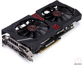
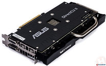
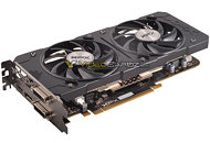
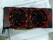
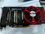
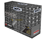
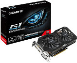
Here are the first pictures of three AIB-branded Radeon R9 380X graphics cards, including one each from ASUS, XFX, and GIGABYTE. The ASUS branded Radeon R9 380X graphics card, the R9 380X STRIX, features the company's dual-slot, dual-fan DirectCU II cooling solution. ASUS is also giving it a slick back-plate, and offering it in two variants based on factory-overclock (or lack of it).

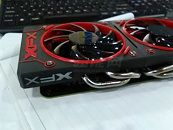
The XFX branded R9 380X features a similar product size to the ASUS card, featuring a moderately long PCB, and a dual-slot, dual-fan "Double Dissipation" cooler. XFX will sell variants of this card in reference and factory-overclocked speeds. Lastly, there's GIGABYTE. Like the others, this card features a medium-size PCB, with the company's dual-slot WindForce 2X cooling solution. Based on the 28 nm "Tonga" aka "Antigua" silicon, the R9 380X reportedly features 2,048 GCN 1.2 stream processors, 128 TMUs, 32 ROPs, and a 256-bit wide GDDR5 memory interface, holding 4 GB of memory. It's expected to launch later this week.
Souces: VideoCardz, HardwareInfo, WCCFTech

AMD Pro A12 "Carrizo" Chip Offers TDP as Low as 12W

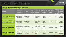
AMD's "Excavator" module could fetch big power dividends for the company, with the top of the line Pro A12 "Carrizo" APU for mobile platforms offering TDP as low as 12W (normal usage), going up to 35W (maximum stress). AMD allows users to set the TDP for their processors. Built on the existing 28 nm process, these chips offer TDPs as low as the ones offered by Intel, built on 22 nm and even 14 nm nodes.

This is made possible because "Excavator" features heavily compacted registers and decode engines, and AMD spent a lot of R&D kicking out redundant or useless components from the silicon. The recently launched A-Series Pro "Carrizo" APUs feature two "Excavator" modules (four CPU cores), a GPU with eight GCN 1.2 compute units (512 stream processors), 2 MB of total cache, dual-channel DDR3-2133 integrated memory controllers.

AMD Readies Radeon R9 380X, XFX Ready with Card

AMD is readying a new SKU to take advantage of the vast pricing gap between the GeForce GTX 960 and GTX 970, and to bolster its sub-$300 lineup, with the Radeon R9 380X. This SKU will be based on the 28 nm "Tonga" silicon, which implements the latest Graphics CoreNext 1.2 architecture. The R9 380X could max out the specifications of the "Tonga" silicon, offering 2,048 stream processors spread across 32 compute units, 128 TMUs, 32 ROPs, and a 384-bit wide GDDR5 memory interface, holding either 3 GB or 6 GB of memory.

Another equally plausible theory pins the R9 380X as a chip with 2,048 stream processors, but the same 256-bit GDDR5 memory interface of the R9 380, with 4 GB of memory, letting AMD keep the costs low. XFX appears to be ready with a "Double Dissipation" card based on the R9 380X. The card's new-generation Double Dissipation cooler features an aluminium fin-stack heatsink with four 8 mm thick nickel-plated copper heat pipes, and a pair of 100 mm spinners, which are easily detachable, letting you clean the heatsink underneath. Mass-production of the R9 380X is reportedly underway, so a launch is to be expected rather soon.

NVIDIA Readies GeForce GTX 950 Ti Mid-range Graphics Card

NVIDIA is preparing to cement its sub-$150 product offering, and compete with AMD's Radeon R7 370, with a new SKU called the GeForce GTX 950 Ti. This chip will succeed the GTX 750 Ti and is expected to be based on the 28 nm "GM206" silicon. The SKU reportedly features an ASIC variant code "GM206-250" (the GTX 960 features "GM206-300.") NVIDIA could create the SKU by either cutting down the CUDA core count (which is 1,024 on the silicon), lowering clock-speeds, or a combination of the two. The chip already features a narrow 128-bit GDDR5 memory interface, compared to the 256-bit memory bus on its competing R7 370.

AMD Also Announces Radeon R9 380 Performance-segment Graphics

In addition to the Radeon R7 300 series, AMD announced the Radeon R9 380 performance-segment graphics card. Available in 2 GB and 4 GB variants, with the 2 GB variant priced at $199, to compete with NVIDIA's GeForce GTX 960, and the 4 GB variant about $50 costlier, the card can play any of today's games at 1080p, with eye-candy maxed out, but can also play them at 1440p, with reasonably high settings.

Based on the 28 nm "Tonga" silicon, the R9 380 packs 1,792 stream processors based on the latest GCN 1.2 architecture, with 112 TMUs, 32 ROPs, and up to 4 GB of memory across a 256-bit wide memory interface. Its core is clocked at 970 MHz, with the memory at 5.70 GHz (GDDR5 effective), churning up 184 GB/s of memory bandwidth. The card's typical power draw is rated at 190W, it draws power from a pair of 6-pin PCIe power connectors.

NVIDIA Announces the GeForce GTX 980 Ti Graphics Card

NVIDIA announced the GeForce GTX 980 Ti, its latest high-end graphics processor. Positioned a notch below the GTX Titan X, and above the GTX 980, it is designed to offer playable frame-rates at 4K Ultra HD resolution, with high-levels of visual details. Based on the same 28 nm GM200 silicon as the GTX Titan X, the chip features 2,816 CUDA cores, carved out by disabling 2 of the 24 streaming multiprocessor units on the silicon; 176 TMUs, 96 ROPs, and a 384-bit wide GDDR5 memory interface, holding 6 GB of memory.

The GeForce GTX 980 Ti features nearly identical clock speeds to the GTX Titan X, with 1000 MHz core, 1076 MHz GPU Boost, and 7012 MHz (GDDR5-effective) memory. The TDP is rated at 250W. The reference design card draws power from a combination of 6-pin and 8-pin PCIe power connectors. Display outputs include three DisplayPort 1.2, and one each of HDMI 2.0 and DVI connectors. The card is capable of 4-way SLI. NVIDIA board partners will launch custom-design variants of this card, with factory-overclocked speeds, and custom air- and liquid-cooled designs. It starts at US $649.99. With this launch, NVIDIA cut prices of the GeForce GTX 980 to $499.99.

AMD Cuts Prices of Radeon R9 285

As the Spring PC upgrade season heats up, AMD decided to woo mainstream gamers away from NVIDIA's GeForce GTX 960, by working with retailers in the EU to introduce price-cuts on its Radeon R9 285 graphics card. The card can now be had for under 180€ (incl taxes). The GTX 960, in comparison, starts at 192€ (incl taxes). The R9 285 offers higher performance than the GTX 960. It is, however, let down by higher power consumption and noise figures. Based on the 28 nm "Tonga" silicon, the R9 285 offers 1,792 stream processors based on AMD's Graphics CoreNext 1.2 architecture, 112 TMUs, 32 ROPs, and a 256-bit wide memory interface, holding 2 GB of memory.

AMD Readying "Godavari" APUs for May Launch, 14 nm APUs in 2016

AMD is readying its next-gen APUs, codenamed "Godavari" for launch in May 2015, according to industry sources in Taiwan. A successor to "Kaveri," Godavari will feature updated "Excavator" architecture based CPU cores, and the latest Graphics CoreNext 1.2 based stream processors on the integrated GPU. The APU will feature PCI-Express gen 3.0 and high-speed DDR3 integrated memory controllers, just like its predecessor "Kaveri," and could be based on the existing FM2+ platform. These chips will compete against some of the entry/mainstream variants of Intel's Core "Broadwell" processors. It's likely that these chips could be built on existing 28 nm process.

It's also being reported that AMD will launch its first APUs based on the 14 nanometer fab process, codenamed "Summit Ridge," in 2016. These will be succeeded by "Raven Ridge" APUs in 2017. AMD could use Samsung and GlobalFoundries to make its 14 nm chips. Lastly, AMD is reportedly in talks with ASMedia to integrate its USB 3.1 controller logic into its new motherboard chipset, which it plans to launch in September 2015.

GIGABYTE Intros its GeForce GTX 960 ITX Graphics Card

GIGABYTE rolled out its latest GeForce GTX 960, designed for space-constrained builds, the GV-N960IX-2GD. This full-height graphics card is just 18.1 cm long, and should squeeze into most compact cubical ITX cases. It features a custom-design PCB that draws power from a single 6-pin PCIe power connector; mated to a compact single-fan cooling solution, which uses a single 90 mm fan to ventilate a dense aluminium fin heatsink, to which heat drawn directly from the GPU die is fed by a pair of 8 mm thick copper heat pipes.

The card offers out of the box clock speeds of 1127 MHz core, 1178 MHz GPU Boost, and 7.00 GHz memory (all reference), and features 2 GB of GDDR5 memory across the chip's 128-bit wide memory interface. Display outputs include a pair of dual-link DVI connectors, and one each of HDMI 2.0 and DisplayPort 1.2. Based on the 28 nm GM206 silicon, the GeForce GTX 960 features 1,024 CUDA cores based on the "Maxwell" architecture. The company didn't announce pricing or availability information.

NVIDIA GeForce GTX TITAN-X Specs Revealed

NVIDIA's GeForce GTX TITAN-X, unveiled last week at GDC 2015, is shaping up to be a beast, on paper. According to an architecture block-diagram of the GM200 silicon leaked to the web, the GTX TITAN-X appears to be maxing out all available components on the 28 nm GM200 silicon, on which it is based. While maintaining the same essential component hierarchy as the GM204, the GM200 (and the GTX TITAN-X) features six graphics processing clusters, holding a total of 3,072 CUDA cores, based on the "Maxwell" architecture.

With "Maxwell" GPUs, TMU count is derived as CUDA core count / 16, giving us a count of 192 TMUs. Other specs include 96 ROPs, and a 384-bit wide GDDR5 memory interface, holding 12 GB of memory, using 24x 4 Gb memory chips. The core is reportedly clocked at 1002 MHz, with a GPU Boost frequency of 1089 MHz. The memory is clocked at 7012 MHz (GDDR5-effective), yielding a memory bandwidth of 336 GB/s. NVIDIA will use a lossless texture-compression technology to improve bandwidth utilization. The chip's TDP is rated at 250W. The card draws power from a combination of 6-pin and 8-pin PCIe power connectors, display outputs include three DisplayPort 1.2, one HDMI 2.0, and one dual-link DVI.

ZOTAC Unveils a Pair of 4 GB GeForce GTX 960 Graphics Cards

ZOTAC joined the 4 GB GeForce GTX 960 party with two factory-overclocked models. The ZT-90308-10M features a minor overclock of 1177 MHz core, with 1240 MHz GPU Boost (vs. reference clocks of 1126/1178 MHz); while the AMP! variant (ZT-90309-10M) offers higher 1266 MHz core with 1329 MHz GPU Boost. The memory clock is untouched on both cards, at 7.00 GHz (GDDR5-effective).

The ZT-90308-10M features a more cost-effective dual-fan cooling solution, while the AMP! offers a meatier dual-fan one. Both cards draw power from single 8-pin PCIe power connectors, and come with back-plates. Display outputs on both include three DisplayPort 1.2, one HDMI 2.0, and one DVI. Based on the 28 nm GM206 silicon, the GTX 960 features 1,024 CUDA cores, 64 TMUs, 32 ROPs, and a 128-bit wide GDDR5 memory interface. ZOTAC didn't announce pricing or availability information.
More pictures follow.

NVIDIA GeForce GTX TITAN-X Pictured Up-close

Here are some of the first close-up shots of NVIDIA's new flagship graphics card, the GeForce GTX TITAN-X, outside Jen-Hsun Huang's Rafiki moment at a GDC presentation. If we were to throw in an educated guess, NVIDIA probably coined the name "TITAN-X" as it sounds like "Titan Next," much like it chose "TITAN-Z" as it sounds like "Titans" (plural, since it's a dual-GPU card). Laid flat out on a table, the card features an a matte-black colored reference cooling solution that looks identical to the one on the original TITAN. Other cosmetic changes include a green glow inside the fan intake, the TITAN logo, and of course, the green glow on the GeForce GTX marking on the top.

The card lacks a back-plate, giving us a peek at its memory chips. The card features 12 GB of GDDR5 memory, and looking at the twelve memory chips on the back of the PCB, with no other traces, we reckon the chip features a 384-bit wide memory interface. The 12 GB is achieved using twenty-four 4 Gb chips. The card draws power from a combination of 8-pin and 6-pin power connectors. The display I/O is identical to that of the GTX 980, with three DisplayPorts, one HDMI, and one DVI. Built on the 28 nm GM200 silicon, the GTX TITAN-X is rumored to feature 3,072 CUDA cores. NVIDIA CEO claimed that the card will be faster than even the previous generation dual-GPU flagship product by NVIDIA, the GeForce GTX TITAN-Z.
Return to Keyword Browsing
Nov 23rd, 2024 06:41 EST change timezone

New Forum Posts

Popular Reviews

Controversial News Posts