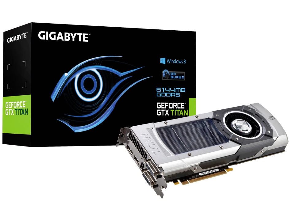
News Posts matching #28 nm

Return to Keyword Browsing

AMD Radeon HD 8000M Series Codenamed "Solar System," To Debut at CES

It was high time AMD updated its tiny entry-thru-mid GPU silicons to the new 28 nm fab process, Graphics CoreNext micro-architecture, and make them truly Windows 8-ready with DirectX 11.1 support. What better way to do those by giving them as big a launchpad as Radeon HD 8000M series branding, and a gala launch at the 2013 International CES? AMD's next-generation mobile GPUs are codenamed "Solar System," breaking away from the desktop GPU family codename of "Sea Islands." Among its members are those named after our planetary neighbours, "Mars" and "Venus," to name a few. The recent leak of a ASUS Vivobook featuring HD 8550M may not be a re-brand, after all.

Leadtek Intros WinFast GeForce GTX 660 Hurricane II Graphics Card

Leadtek rolled out the WinFast GeForce GTX 660 Hurricane II graphics card. Based around the same cooler design as its recently-launched WinFast GTX 650 Ti Hurricane II, the card uses a non-reference design PCB, augmented with the company's dual-fan Hurricane II GPU cooler.

The WinFast GTX 660 Hurricane II features reference clock speeds of 980 MHz core, 1033 MHz GPU Boost, and 6.00 GHz memory (GDDR5-effective). It features 2 GB of memory across a 192-bit wide memory interface. Based on the 28 nm GK106 silicon, the GeForce GTX 660 packs 960 CUDA cores. The card draws power from a single 6-pin power connector, display outputs include two DVI, and one each of HDMI and DisplayPort.

Sapphire Also Launches a China-Exclusive Radeon HD 7750 OC Graphics Card

In addition to the global launch of Vapor-X CPU cooler, Sapphire rolled out a factory-overclocked Radeon HD 7750 OC Edition graphics card that's exclusive to the Greater China region. The card is based on the standard cost-effective full-height board design Sapphire used on the base model, enhanced with a factory-overclock of 850 MHz core, with 4.80 GHz memory. It packs 1 GB of GDDR5 memory across a 128-bit wide memory interface. Based on the 28 nm "Cape Verde" silicon, the Radeon HD 7750 packs 512 Graphics CoreNext stream processors. It is expected to be priced around 650 RMB.

Samsung to Unveil 4+4 Core big.LITTLE Processor in 2013

Samsung is reportedly taking interest in ARM's big.LITTLE technology - an SoC design in which high-performance Cortex-A15 cores are combined by low-power Cortex-A7 cores, and the two are made to trade places as the device's CPU, depending on the load. An SoC slated for 2013, which could probably feature in high-end smartphones and tablets, sees a combination of four each of A15 and A7 cores. The A15 cores are clocked at 1.80 GHz, and A7 at 1.20 GHz, with the former featuring higher IPC than the latter. A 2 MB last-level cache serves as town-square for data and instructions going to the various cores. The chip will be built on the 28 nm process.

MSI Intros Low-Profile GeForce GT 640 Graphics Card with Three Display Outputs

MSI announced a new low-profile, single slot graphics card based on the GeForce GT 640 (model: N640GT-MD2GD3/LP). The card gives users the advantage of support for 3-display 3DVision Surround, for productivity. It packs 2 GB of DDR3 memory across a 128-bit wide interface, to aid with smooth display on those three monitors. It ships with 900 MHz core, and 1792 MHz memory (DDR). Display outputs include one each of dual-link DVI, HDMI, and D-Sub. Based on the 28 nm GK107 silicon, the GeForce GT 640 packs 384 CUDA cores. The new card is expected to be priced around US $90.

AMD Third-Generation APUs to be Built on 28 nm Process

A leaked company roadmap slide revealed that AMD's third-generation performance APU, codenamed "Kaveri," will be built on the 28 nm silicon fabrication process. The chips will be built by Global Foundries. Kaveri combines AMD's next-generation CPU architecture codenamed "Steamroller" with Graphics CoreNext GPU architecture.

In addition to Kaveri, AMD will introduce a major update to its low-power APU lineup with "Kabini." A true successor to "Brazos," Kabini features x86-64 cores built on the energy-optimized "Jaguar" architecture (which succeeds "Bobcat," on which Brazos APUs are built). It is also mentioned that Kabini will be a true system-on-chip (SoC), with integration of the FCH chipset into the APU silicon. Such an integration could increase die size and complexity, but could also minimize the board footprint of the platform, making it possible to use the SoC in thin tablets, and COMs.

Tesla K20 GPU Compute Processor Specifications Released

Specifications of NVIDIA's Tesla K20 GPU compute processor, which was launched way back in May, are finally disclosed. We've known since then that the K20 is based on NVIDIA's large GK110 GPU, a chip never used to power a GeForce graphics card, yet. Apparently, NVIDIA is leaving some room on the silicon that allows it to harvest it better. According to a specifications sheet compiled by Heise.de, Tesla K20 will feature 13 SMX units, compared to the 15 available on the GK110 silicon.

With 13 streaming multiprocessor (SMX) units, the K20 will be configured with 2,496 CUDA cores (as opposed to 2,880 physically present on the chip). The core will be clocked at 705 MHz, yielding single-precision floating point performance of 3.52 TFLOP/s, and double-precision floating point performance of 1.17 TFLOP/s. The card packs 5 GB of GDDR5 memory, with memory bandwidth of 200 GB/s. Dynamic parallelism, Hyper-Q, GPUDirect with RDMA are part of the new feature-set. The TDP of the GPU is rated at 225W, and understandably, it uses a combination of 6-pin and 8-pin PCI-Express power connectors. Built in the 28 nm process, the GK110 packs a whopping 7.1 billion transistors.

VTX3D Introduces its HD7990 6 GB Graphics Card

A leading brand of graphics card maker - VTX3D, today unrolls the VTX3D HD7990, serving PC enthusiastic with most extreme gaming performance. The HD7990 utilizes the advanced 28 nm architecture and PCIE 3.0 design to maximize GPU performance, even allowing greater OC ability with dual BIOS switch button embedded on bracket, which offers default mode and OC mode to choose, showing the most unrivaled performance than ever.

Fitted with 6 GB of GDDR5 memory connected via high speed 384bit x2 memory interface, VTX3D HD7990 is clocked at 900 MHz by default setting and 925 MHz at OC mode, both together with 1375 MHz for memory, revealing monster-like power for the most demanding games. The HD7990 also features ultra deluxe design with digital PWM, multi phases design and UHB, ensuring stability and reliability voltage for GPU with minimum conduction losses and lower temperatures at load.

ARM Announces POP IP Technology for Mali-T600 Series GPUs

ARM today introduced the first POP IP solution for ARM Mali-T600 series graphics processor units (GPUs). This latest offering of POP IP -- core-hardening acceleration technology that produces the best implementations of ARM processors in the fastest time-to-market -- is optimized for the Mali-T628 and Mali-T678 on TSMC 28 nm HPM process technology. Mali GPUs go into a variety of end devices, including a wide range of smartphones, from high performance to mass market, as well as tablets and smart TVs. It is critical that designers can optimize their Mali GPU for their selected end applications.

Developed in synergistic collaboration by ARM's Media Processing and Physical IP divisions, the optimized POP IP technology has been created to produce the most efficient GPU implementations at 28 nm. The POP IP enabled Mali-T600 series GPU implementation results in superior performance density/watt, and significant silicon savings. Benefits of this POP IP have been proven to deliver up to 27 percent higher frequency, 24 percent lower area, and 19 percent lower power than implementations which do not use POP IP.

PNY Announces XLR8 GeForce GTX 650 Ti Graphics Card

PNY announced its XLR8 GeForce GTX 650 Ti graphics card. Based on an identical board design to Palit's offering, the card is likely originally manufactured by it. The XLR8 GTX 650 Ti features near-reference clock speeds, of 928 MHz core, and 5.40 GHz (GDDR5-effective) memory. It packs 1 GB of GDDR5 memory across a 128-bit wide memory interface. The card uses an aluminum fin heatsink that's ventilated by an 80 mm fan. Based on the 28 nm GK106 ASIC, the GTX 650 Ti packs 768 CUDA cores, 64 TMUs, and 16 ROPs. PNY's offering includes download coupons to five movies, and a 3-month subscription to E-Sports Entertainment (ESEA) Premium Video Game Network. It is priced at US $179.99.

Club 3D Radeon HD 7990 Graphics Card Pictured

Club 3D plans to be one of the very few AMD AIB partners with a Radeon HD 7990 dual-GPU graphics card. Its product is based on the same exact design as PowerColor's recently-launched HD 7990 base and flagship HD 7990 Devil13, since TUL (PowerColor's parent company) is the OEM of Club 3D Radeon series graphics cards. The card packs two 28 nm "Tahiti" Radeon HD 7970 ASICs with a PLX-made PCI-Express 3.0 bridge chip, and a total of 6 GB of GDDR5 memory across two 384-bit wide memory interfaces. It's likely that Club 3D's card sticks to the same clock profiles as PowerColor's HD 7990 base, with 900 MHz core, 925 MHz OC (toggled manually with a switch), and 5.50 GHz memory. More details are awaited.

GeForce GTX 650 Ti Final Specifications Out

Sources among retailers confirmed what could be the finalized specifications of NVIDIA's upcoming GeForce GTX 650 Ti graphics processor. Some of these specifications were first leaked when Newegg.com accidentally listed Galaxy GTX 650 Ti GC. According to the sources, the GTX 650 Ti, which is based on the 28 nm GK106 silicon, will carry the ASIC label "GK106-220," it will be configured with 768 CUDA cores (and not 576, as earlier believed).

GeForce GTX 650 Ti will have a narrower 128-bit wide GDDR5 memory interface, holding 1 GB of memory. The source also revealed NVIDIA-reference clock speeds to be 925 MHz core, with 1350 MHz (5.40 GHz GDDR5-effective) memory, churning up 86.4 GB/s memory bandwidth. The chip's TDP is rated at 110W, and cards based on it feature one 6-pin PCIe power connector. According to older reports, the GTX 650 Ti is slated for October 9.

Samsung and STMicroelectronics Enter Strategic Relationship for 32 nm and 28 nm Tech

Samsung Electronics, Co., Ltd., a world leader in advanced semiconductor technology solutions, announced foundry production of STMicroelectronics' leading products using 32/28nm High-K Metal Gate (HKMG) process technology. Samsung Electronics' foundry business has been selected by STMicroelectronics to provide it with products at the 32/28nm process node. The relationship has already resulted in taping-out of a dozen ST advanced system-on-chip (SoC) devices for mobile, consumer and network applications.

"We have successfully started production of STMicroelectronics' new-generation 32/28nm SoC products," said Kwang-Hyun Kim, executive vice president of Foundry business, Device Solutions, Samsung Electronics. "A foundry relationship with ST demonstrates our commitment to advanced process technology and our 32/28nm HKMG process-technology leadership. We have aggressively ramped 32/28nm capacity and will continue to deliver the most advanced process solutions to our customers."

MSI GeForce GTX 660 HAWK Graphics Card Detailed

MSI's flagship factory-overclocked graphics card based on the GeForce GTX 660, the N660GTX HAWK, was pictured and detailed by Expreview, earlier this week. According to the source, the card will be designed for about 15% higher core clock speeds than reference, backed by high-grade voltage regulation circuitry and the company's TwinFrozr IV cooling solution.

To begin with, the GeForce GTX 660 HAWK will ship with clock speeds of 1100 MHz core, 1176 MHz GPU Boost core clock speeds. The memory is left untouched at 6.00 GHz (GDDR5-effective). Under the hood is a 10-phase VRM that uses SSC chokes (low energy loss to noise), and IR DirectFETs. The card appears to use a high-end voltage controller that allows software voltage control, and consolidated voltage measurement points. The card draws power from two 6-pin PCIe power connectors.

AMD "Oland" Radeon HD 8800 Series SKUs Unveiled

Apparently, launch of AMD's Radeon HD 8800 series is close enough for some sources to come up with specifications. The HD 8800 series, according to one source, is based on a new silicon codenamed "Oland," which is built on the 28 nm process, packing 3.4 billion transistors with around 270 mm² die-area. According to the source, the two HD 8800 series models, the HD 8870 "Oland XT" will up performance per Watt and cost-performance ratios over current HD 7800 series, while maintaining current process technologies.

The Radeon HD 8870, according to numbers provided by the source, could offer performance comparable to today's high-end GPUs. The HD 8870 is clocked at 1050 MHz with 1100 MHz PowerTune Boost frequency; while the HD 8850 is clocked at 925 MHz with 975 MHz boost frequency. The memory of both SKUs is clocked at 6.00 GHz, yielding 192 GB/s memory bandwidth. The chips hence have 256-bit wide memory interfaces.

Point of View Completes 'Kepler' Line with GeForce GTX 650 and GeForce GTX 660

Point of View, a premier NVIDIA graphics partner and manufacturer of Android tablets, notebooks and other hardware, launches today two new cards of the GeForce 600 family: the POV GeForce GTX 660 and the POV GeForce GTX 650.

The current GeForce 600 range is truly the next step in computer graphics. The differences in performance compared to previous generation are so huge that - not - upgrading is a shame.

Sparkle Announces the Calibre X680/X670 Captain Graphics Cards

Calibre, one of industry leading brands of graphics solutions, launches the latest products, Calibre X680 Captain & Calibre X670 Captain, powered by NVIDIA's TOP 28 nm Kepler engine - GK104.

Calibre Series Returns with Maximum Performance

As the flagship product line of Calibre, Captain Series brings the tremendous different from reference design by tweaking the performance and cooling system, bringing the tremendous different from reference design. Moreover, Calibre X680/ X670 Captain Series preloaded overclocking value for enthusiasts.

MSI Announces Radeon HD 7750 OC V2 Graphics Card

MSI announced a the R7750 OC V2, a new factory-overclocked graphics card based on the Radeon HD 7750 GPU. The card ships with clock speeds of 830 MHz core, with 4.50 GHz memory. It packs 1 GB of GDDR5 memory across a 128-bit wide interface. Based on the 28 nm "Cape Verde" silicon, it packs 512 Graphics CoreNext stream processors. Unlike the R7750-PMD1GD5/OC, the new OC V2 features a quieter single-fan cooler, which uses a round GPU heatsink with radially-projecting aluminum fins. The new cooler also appears to be cost-effective, giving MSI more room for price-cuts.

ASUS Announces GeForce GTX 660 Ti DirectCu II Graphics Cards

ASUS announced as many as five GeForce GTX 660 Ti graphics card models. The cards are based on the company's dual-slot DirectCu II cooling solution, and a PCB design that's similar to that of the GeForce GTX 670 DirectCu series. Among the five models are the GTX660 TI-DC2-2GD5, the base model that sticks to NVIDIA reference clock speeds of 915/980/6008 MHz (core/boost/memory); the GTX660 TI-DC2O-2GD5, with a mild level of factory-overclocking, at 967/1058/6008 MHz; GTX660 TI-DC2T-2GD5, or TOP variant, with 1059/1377/6008 MHz; and variants of the GTX660 TI-DC2O-2GD5 and GTX660 TI-DC2T-2GD5 that feature Steam coupons to Borderlands 2 game.

Based on the 28 nm GK104 silicon, the GeForce GTX 660 Ti packs 1344 CUDA cores, 112 TMUs, 24 ROPs, and a 192-bit wide memory interface, holding 2 GB of memory. ASUS' cards uses two 6-pin PCIe power connectors to draw power. Display outputs include a pair of dual-link DVI, and one each of HDMI and DisplayPort. The cards are 3-way SLI capable. The DirectCu II cooler uses a compound heatsink to which heat is fed by a number of copper heat pipes, which make direct contact with the GPU. ASUS plans 3 GB variants of the same models, in which six 2 Gbit memory chips make up 3072 MB of memory, with 144 GB/s memory bandwidth.

ARM and GLOBALFOUNDRIES Collaborate to Enable Devices on 20 nm and FinFET

GLOBALFOUNDRIES and ARM today announced a multi-year agreement to jointly deliver optimized system-on-chip (SoC) solutions for ARM processor designs on GLOBALFOUNDRIES' 20-nanometer (nm) and FinFET process technologies. The new agreement also extends the long-standing collaboration to include graphics processors, which are becoming an increasingly critical component in mobile devices. As part of the agreement, ARM will develop a full platform of ARM Artisan Physical IP, including standard cell libraries, memory compilers and POP IP solutions. The results will help enable a new level of system performance and power-efficiency for a range of mobile applications, from smartphones to tablets to ultra-thin notebooks.

The companies have been collaborating for several years to jointly optimize ARM Cortex-A series processors, including multiple demonstrations of performance and power-efficiency benefits on 28nm as well as a 20nm test-chip implementation currently running through GLOBALFOUNDRIES fab in Malta, N.Y. This agreement extends the prior efforts by driving production IP platforms that will enable customer designs on 20nm and promote rapid migration to three-dimensional FinFET transistor technology. This joint development will enable a faster time to delivering SoC solutions for customers using next-generation ARM CPUs and GPUs in mobile devices.

ELSA Announces GeForce GT 640 2 GB Graphics Card

ELSA announced a new 2 GB GeForce GT 640 graphics card in the full-height, single-slot form-factor (model: GD640-2GERGT). The card uses an aluminum fan-heatsink that stays within the confines of a single expansion card slot. The card sticks to NVIDIA reference clock-speeds for the GeForce GT 640, of 900 MHz core and 1.78 GHz memory. The card packs 2 GB of GDDR3 memory installed across a 128-bit wide memory interface. The 28 nm GK107 silicon packs 384 CUDA cores. The card draws power from the PCI-Express slot. Display outputs include two dual-link DVI and a mini-HDMI. It is slated for mid-August.

GeForce GTX 650 Ti Specifications Detailed

A little earlier this week, specifications of NVIDIA's GeForce GTX 650 graphics processor were reported. An even newer report by DonanimHaber details its sibling, the GeForce GTX 650 Ti, designed for the sub-$250 market. The new GPU is based on the NVIDIA's newest GK106 silicon, while the GTX 650 sticks to the GK107, and is essentially a beefed-up GeForce GT 640. These are the specifications of the GeForce GTX 650 Ti we're looking at:
  • 28 nm GK106 silicon
  • 960 CUDA cores
  • 192-bit wide GDDR5 memory interface
  • 1 GB and 2 GB memory options
  • Q4-2012 launch

NVIDIA GeForce GTX 650 Specifications and Launch Date Leaked

Following the launch of its GeForce GTX 660 series graphics processors, NVIDIA is likely to turn its attention to the sub-$200 market, particularly in the crucial back-to-school shopping season, with the launch of the new GeForce GTX 650 graphics processor. The new chip will help the company capture a key sub-$200 price-point, and replace the GeForce GTX 550 Ti.

According to a DonanimHaber report, the GeForce GTX 650 will be based on the new 28 nm GK107 ASIC, which is derived from the GeForce Kepler architecture. The chip will pack 384 CUDA cores, and a 128-bit wide GDDR5 memory interface, which holds 1 GB of memory. The same report pin-points the launch date to 17th September.

GeForce GTX 660 Ti Specifications and Launch Date Released

According to the latest set of specifications scored by SweClockers, NVIDIA's upcoming performance-segment GPU, the GeForce GTX 660 Ti, is not much different from the GTX 670. The GTX 660 Ti is based on the 28 nm GK104 GPU, with 1,344 CUDA cores enabled - the same number as that on the GTX 670. What's more, the clock speeds don't differ between the two, either - 915 MHz core, 980 MHz GPU Boost, and 6.00 GHz GDDR5-effective memory.

The memory amount stays 2 GB, as well. It's just that the memory bus width is reduced from 256-bit to 192-bit, resulting in 25% lower memory bandwidth. The 2 GB of memory is spread across the 192-bit memory bus, probably with four chips using 32-bit wide paths each, with four other chips sharing two 32-bit wide paths. NVIDIA is known for pulling off such memory configurations, like it did with the GeForce GTX 550 Ti.

GeForce GTX 660 Arrives Mid-August: Report

NVIDIA's newest product designed to strike the price-performance "sweetspot," the GeForce GTX 660, is set for a mid-August market launch, according to a SweClockers report. The new chip could roll out some time between August 13 and 19. Given that other Kepler-based SKUs have been launched on Tuesdays or Thursdays, it's likely that the launch date could be either the 14th, or the 16th. The GTX 660 will be based on the 28 nm "GK104" GPU. It will feature 1,344 or 1,152 CUDA cores, and a 192-bit wide GDDR5 memory interface, holding 1.5 GB of memory, according to the report. The new GPU could capture a crucial sub-$300 price-point.
Return to Keyword Browsing
Aug 14th, 2024 15:50 EDT change timezone

New Forum Posts

Popular Reviews

Controversial News Posts