Intel's Ponte Vecchio HPC GPU Successor Rialto Bridge Gets the Axe
Late on Friday in a newsroom posting by Intel's Interim GM Jeff McVeigh a roadmap uplift was quietly revealed. Rialto Bridge, the process improved version of Ponte Vecchio currently shipping under the Max Series GPU branding, has been pulled from the roadmap in favor of doubling down on the future design code-named Falcon Shores. Rialto Bridge was first announced last May at SC22 as the direct successor to Ponte Vecchio, and was set to begin sampling later this year. In the same post Intel also cancelled Lancaster Sound, their Visual Cloud GPU meant to replace the Arctic Sound Flex series of GPUs based on similar Xe cores to Arc Alchemist. In its stead the follow-up architecture Melville Sound will receive focused development efforts.
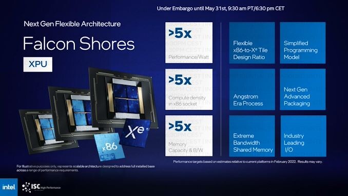
Falcon Shores is described as a new foundational chiplet architecture that will integrate more diverse compute tiles, creating what Intel originally dubbed the XPU. This next architectural step would combine what Intel is already doing with products such as Sapphire Rapids and Ponte Vecchio into one CPU+GPU package, and would offer even further flexibility to add other kinds of accelerators. With this roadmap update there is some uncertainty as to whether the XPU designation will make the transition as it is notably absent in the letter. It is clear though that Falcon Shores will directly replace Ponte Vecchio as the next HPC GPU, with or without CPU tiles included.

Falcon Shores is described as a new foundational chiplet architecture that will integrate more diverse compute tiles, creating what Intel originally dubbed the XPU. This next architectural step would combine what Intel is already doing with products such as Sapphire Rapids and Ponte Vecchio into one CPU+GPU package, and would offer even further flexibility to add other kinds of accelerators. With this roadmap update there is some uncertainty as to whether the XPU designation will make the transition as it is notably absent in the letter. It is clear though that Falcon Shores will directly replace Ponte Vecchio as the next HPC GPU, with or without CPU tiles included.