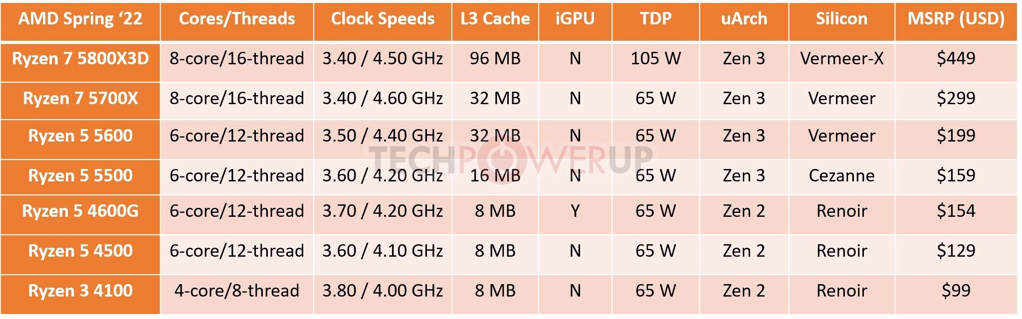
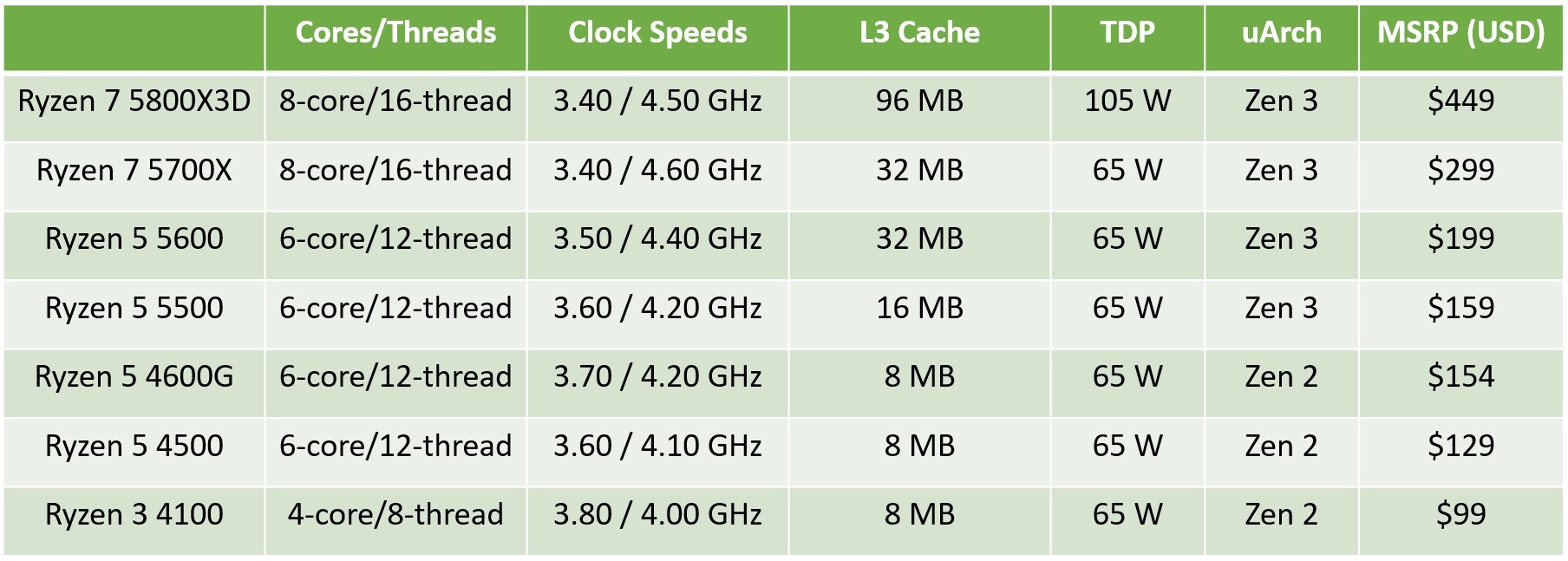
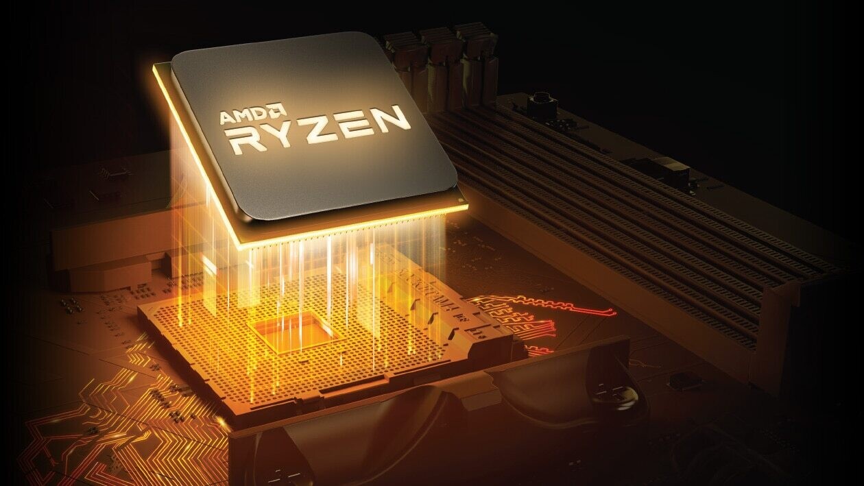
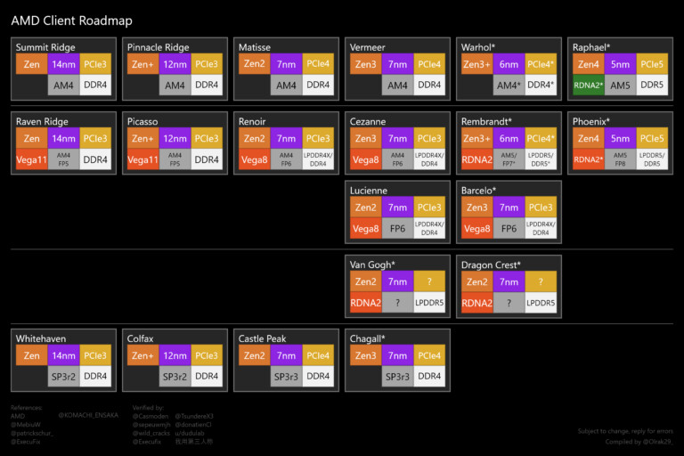
AMD Readies a Handful New Ryzen PRO 5000 Desktop Processor SKUs
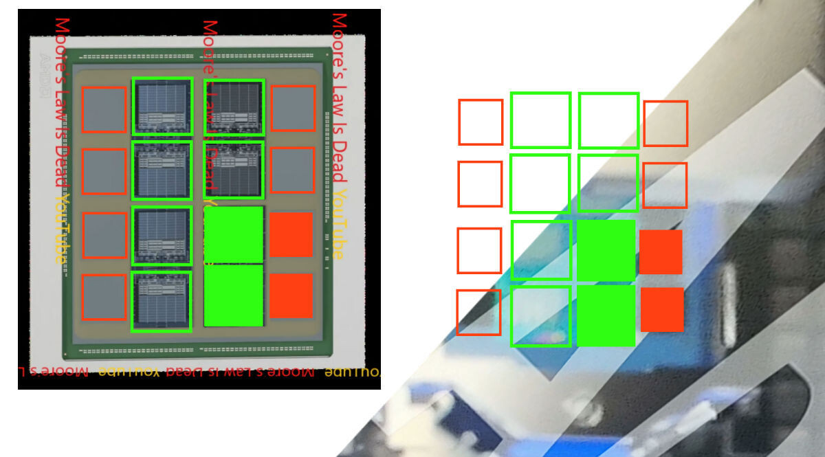
AMD is readying a handful new Ryzen PRO 5000 series desktop processor models, according to a leaked Lenovo datasheet for commercial desktops. These Socket AM4 processors are based on either the 7 nm "Renoir" monolithic silicon with "Zen 2" CPU cores; or the "Vermeer" MCM with "Zen 3" cores; all feature 65 W TDP, and the AMD PRO feature-set that rivals Intel vPro, including a framework for remote management, AMD PRO Security, PRO Manageability, and PRO Business (a priority tech-support channel).
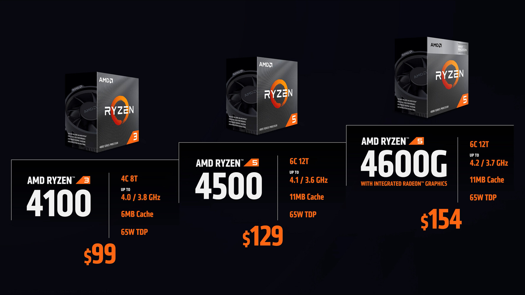
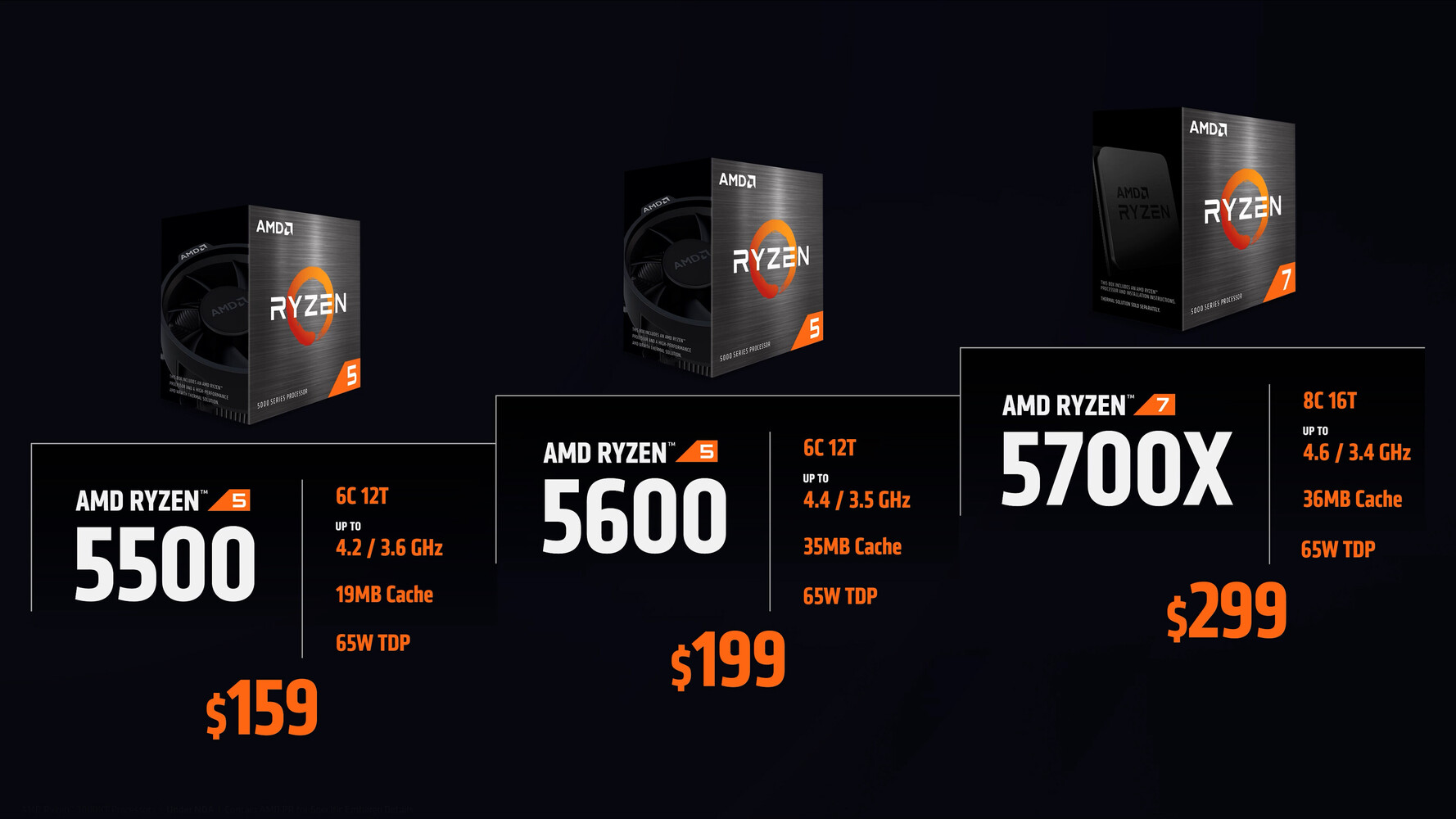
Models in the lineup include the Ryzen 3 PRO 4350G, a "Renoir" based APU with a 4-core/8-thread "Zen 2" CPU clocked up to 4.00 GHz, and Radeon Vega 6 integrated graphics. The Ryzen 5 PRO 5645 is based on "Vermeer," and is a 6-core/12-thread "Zen 3" processor with 32 MB of L3 cache, and up to 4.60 GHz clock speeds. The Ryzen 7 PRO 5845 is the 8-core/16-thread model in the lineup, clocked up to 4.60 GHz. Leading the pack is the Ryzen 9 5945, a 12-core/24-thread chip clocked up to 4.70 GHz. From the looks of it, these processors will be exclusively available in the OEM channel, but AMD's OEM-only chips inevitably end up in the retail channel where they're sold loose from trays.
Models in the lineup include the Ryzen 3 PRO 4350G, a "Renoir" based APU with a 4-core/8-thread "Zen 2" CPU clocked up to 4.00 GHz, and Radeon Vega 6 integrated graphics. The Ryzen 5 PRO 5645 is based on "Vermeer," and is a 6-core/12-thread "Zen 3" processor with 32 MB of L3 cache, and up to 4.60 GHz clock speeds. The Ryzen 7 PRO 5845 is the 8-core/16-thread model in the lineup, clocked up to 4.60 GHz. Leading the pack is the Ryzen 9 5945, a 12-core/24-thread chip clocked up to 4.70 GHz. From the looks of it, these processors will be exclusively available in the OEM channel, but AMD's OEM-only chips inevitably end up in the retail channel where they're sold loose from trays.