News Posts matching #Zen 2

Return to Keyword Browsing

AMD Prepares 7nm "Renoir X" Processors Lacking Integrated Graphics, and "Vermeer S"

AMD apparently finds itself with quite a bit of undigested 7 nm "Renoir" silicon, which it plans to repackage as Socket AM4 processors, reports VideoCardz, citing sources on ChipHell forums. The most interesting aspect of this leak is that the silicon variant, codenamed "Renoir X," comes with a disabled iGPU. This is hence a case of AMD harvesting enough "Renoir" dies with faulty iGPU components, to sell them off as desktop processors. It is also learned that these chips don't feature all of the 8 "Zen 2" CPU cores present on the silicon, but rather AMD is looking to carve out entry-level SKUs, such as the Ryzen 3 or Athlon. The company lacks Athlon desktop SKUs based on "Zen 2" or later, although traditionally the company sought to include some basic iGPU solution with its Athlon SKUs.

In related news, the source reports that AMD will refresh its Ryzen desktop processor family with the new "Vermeer S" Ryzen processors. Built on the existing Socket AM4 package, these use AMD's "Zen 3" CCDs that feature 3D Vertical Cache (3DV Cache), much like the recently announced EPYC "Milan X" server processors. AMD claimed that the 3DV Cache technology has a significant performance uplift on performance akin to a generational update. These could be the company's first response to Intel Core "Alder Lake," although since they're based on the older AM4 platform, could only feature DDR4 and PCIe Gen 4. Much like the Ryzen 3000XT series, these appear to be a stopgap product lineup, with AMD targeting late-Q2/early-Q3 for next-generation "Raphael" Socket AM5 processors based on the "Zen 4" architecture, with DDR5 and PCIe Gen 5.

AMD Celebrates 5 Years of Ryzen...and Insomnia at Intel

AMD disrupted a decade of $350 quad-core from Intel with its path-breaking Ryzen processor and the "Zen" microarchitecture, which enters 5th year in the market (5 years since tapeout). AMD went into the Ryzen processor launch as a company that had been written off in the CPU space by PC enthusiasts, and "Zen" was at best expected to give AMD another round of processors to sell around $250. Boy was everyone wrong. The Ryzen 7 1800X eight-core processor brought HEDT-levels of performance to the mainstream desktop form-factor, and its HEDT counterpart, the Threadripper, dominated Intel's Core X series ever since.
Intel's first response to the 1800X was a 50% increase in CPU core counts calculating that AMD would only see marginal IPC increases going forward, and the superior IPC of "Skylake" cores, along with a 6-core/12-thread setup in the Core i7-8700K would see things through. This is roughly when Intel faced severe supply shortages that spiraled prices out of control, giving AMD space to come out with the Ryzen 7 2700X with a 4% IPC increase, and improved multi-threaded performance, but more importantly, predictable pricing at around $330. Months later, Intel refreshed its lineup with the 9th Gen, and finally attained parity with AMD in core counts, with the Core i9-9900K.

Meltdown-like Vulnerability Affects AMD Zen+ and Zen2 Processors

Cybersecurity researchers Saidgani Musaev and Christof Fetzer with the Dresden Technology University discovered a novel method of forcing illegal data-flow between microarchitectural elements on AMD processors based on the "Zen+" and "Zen 2" microarchitectures, titled "Transient Execution of Non-canonical Accesses." The method was discovered in October 2020, but the researchers followed responsible-disclosure norms, giving AMD time to address the vulnerability and develop a mitigation. The vulnerability is chronicled under CVE-2020-12965 and AMD Security Bulletin ID "AMD-SB-1010."

The one-line summary of this vulnerability from AMD reads: "When combined with specific software sequences, AMD CPUs may transiently execute non-canonical loads and store using only the lower 48 address bits, potentially resulting in data leakage." The researchers studied this vulnerability on three processors, namely the EPYC 7262 based on "Zen 2," and Ryzen 7 2700X and Ryzen Threadripper 2990WX, based on "Zen+." They mention that all Intel processors that are vulnerable to MDS attacks "inherently have the same flaw." AMD is the subject of the paper as AMD "Zen+" (and later) processors are immune to MDS as demonstrated on Intel processors. AMD developed a mitigation for the vulnerability, which includes ways of patching vulnerable software.

Find the security research paper here (PDF), and the AMD security bulletin here. AMD's mitigation blueprint can be accessed here.

Scalpers Already "Offering" the Steam Deck for $5,000 on eBay

Valve's Steam Deck announcement took the gaming world by storm last week, as the announcement of a Valve-designed portable gaming console packing an AMD Zen 2 CPU with RDNA2 cores set collective imaginations on fire. However, as is the case for any recent gaming hardware launches, expect the Steam Deck to be hard to come by - demand for a mainstream portable, Switch-like console that promises to enable AAA-gaming on the go is apparently sky-high, despite the fact that some portable devices exploring the same concept have been available for a while now, such as the AYA Neo (which even packs two extra Zen 2 cores) and the Intel-based One XPlayer.

As is the case for any recent hardware launch that garners enough mainstream attention (looking at you, current-gen GPUs and consoles), a lopsided demand-supply ratio is a playground for unscrupulous types looking to make a profit at the expense of other people's impatience. And it sure is happening already - eBay listings for "pre-order confirmed" Steam Deck variants are already being set at €4,324 (roughly $4,989) - though we'd say they're tentatively set at that ludicrous pricing. It seems that the current median asking price sits around the $900 mark for the 512 GB SSD-equipped variant. Tentative or not, this just goes to show that the new normal is for launched products to be actively gauged for scalping practices - more now than ever before.

Valve Steam Deck SoC Detailed: AMD Brings Zen2 and RDNA2 to the Table

Valve today announced its first big splash into the console market with Steam Deck, a device out to eat the Nintendo Switch's lunch. The announcement comes as yet another feather in AMD's cap for its semi-custom SoC business, benefiting from being the only company with an x86-64 CPU license and having a cutting-edge graphics hardware IP. Built on the 7 nm node at TSMC, the semi-custom chip at the heart of the Steam Deck is designed for extended gameplay on battery, and is a monolithic silicon that combines CPU, GPU, and core-logic.

The yet-unnamed semi-custom chip features a 4-core/8-thread CPU based on the "Zen 2" microarchitecture, with a nominal clock speed of 2.40 GHz, and up to 3.50 GHz boost. The CPU component offers an FP32 throughput of 448 GFLOP/s. The GPU is based on AMD's latest RDNA2 graphics architecture—the same one powering the Xbox Series X, PlayStation 5, and Radeon RX 6900 XT—and is comprised of 8 RDNA2 compute units (512 stream processors). The GPU operates at an engine clock speed of 1.10 GHz to 1.60 GHz, with peak compute power of 1.6 TFLOP/s. The silicon uses a unified memory interface, and a cutting-edge LPDDR5 memory controller.

Prebuilts with AMD 4700S Desktop Kits Sell for $600 in India

Indian PC components retailer PrimeABGB started listing pre-built desktops based on the AMD 4700S Desktop Kit, a PC motherboard based on harvested PlayStation 5 SoCs with their iGPUs disabled. These are semi-custom SoCs originally bound for Sony, which didn't make the cut, as their iGPUs were found defective.

It appears like the desktop PrimeABGB is selling for the equivalent of $600, is integrated in-house by the retailer, and the other parts that make up the build are certainly of a comparable quality to the ones large OEMs cram in their $600 desktops. These include a SilverStone Sugo 13 Mesh case, an Antec Atom 450 W PSU, a 120 GB SATA 6 Gbps SSD, and a GeForce GT 710 handling graphics on par with basic iGPU solutions. What you're getting, though, is an 8-core/8-thread "Zen 2" CPU that's highly capable for productivity tasks, and hardwired 16 GB memory.

AMD 4700S 8-core Processor Desktop Kit Listed as an Official AMD Product

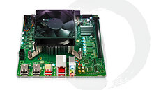
Back in May, pictures surfaced of a curious-looking Micro-ATX motherboard featuring a so-called "AMD 4700S" SoC. At the heart of these boards were an SoC not unlike the one that powers the Xbox Series X, except that the integrated GPU is completely disabled, with no onboard display outputs. The board is very likely a means for AMD to harvest Xbox Series X/S SoCs with broken iGPUs. It now turns out that the board is an official AMD product, named "AMD 4700S 8-core Processor Desktop Kit."

The board provides an 8-core/8-thread CPU based on the "Zen 2" microarchitecture, no iGPU, but a PCI-Express x16 slot that's electrically PCI-Express 2.0 x4, a handful USB 2.0 and USB 3.0 ports, two SATA 6 Gbps ports, onboard 1 GbE LAN and 6-channel HD audio. The SoC comes with its own unspecified amount of onboard memory in the form of hardwired DDR4 memory chips surrounding it; there are no additional memory slots. The Xbox Series X SoC features a 256-bit wide memory bus, so it will be interesting to see if AMD has maximized it. AMD didn't reveal pricing or availability information, although they way this is marketed, the board will very likely be available in the retail channel.

AMD 4700S Processor Could be Repurposed Xbox Series X/S APU

The AMD 4700S is a new processor being advertised by Chinese manufactures as a complete ITX compatible solution. The processor is soldered to a custom "Cardinal" motherboard produced by AMD which lacks memory slots and instead features 16 GB of GDDR6 memory located around the processor. These specifications seem to closely reflect those of the Xbox Series X APU. The 4700S is an 8-core 16-thread 7 nm Zen 2 CPU with 12 MB cache and a boost clock of 4.0 GHz which is actually higher than that of the Xbox Series X/S at 3.8 GHz and 3.6 GHz respectively. This higher boost clock is likely due to the exclusion of an integrated GPU which increases the power available for the processor.

The seller also provided benchmarks for the processor in various Cinebench configurations where it outperformed the Intel Core i7-9700 and performed just below the AMD Ryzen 7 4750G. The processor paired with an RX 550 GPU also outperformed the Intel Core i7-9750H paired with an RTX 2060 and 32 GB memory in Cinebench and x264/x265 video encoding. The seller has a picture of the Xbox Series X APU in their advertising material for the new processor lending weight to the theory that these are reused processors which failed qualification.

AMD Outs 32 MB Infinity Cache on Navi 23, No Cache on Upcoming Van Gogh APUs

AMD has revealed the Infinity Cache size for the upcoming Navi 23 GPU, as well as its absence in the next-generation Van Gogh APU, which features Zen 2 cores and an RDNA GPU. The reveal comes via a new patch done by AMD to the AMKFD, a Linux kernel HSA driver for AMD APUs. The patch file doesn't list Infinity Cache per se, but does clarify the last-level cache for AMD's GPUs - L3, which is essentially the same.

The patch reveals L3 size for Sienna Cichlid (Navi 21), Navy Flounder (Navi 22), and Dimgrey Cavefish (Navi 23). Navi 21 features 128*1024 (128 MB) of Infinity Cache, the just-released Navi 22 has 96 MB, as we know, and according to the file, Navi 23 is bound to feature 32 MB of it. Considering that Van Gogh lacks an infinity Cache, it would seem that it's making use of previous-gen Navi graphics, and won't leverage RDNA2, of which the Infinity Cache is a big part of. It remains to be seen if Van Gogh will materialize in an APU product lineup or if it's a specific part for a customer. It also remains to be seen which RX product will Navi 23 power - if an AMD RX 66000 series, or 6500 series.

AMD's Next-Generation Van Gogh APU Shows Up with Quad-Channel DDR5 Memory Support

AMD is slowly preparing to launch its next-generation client-oriented accelerated processing unit (APU), which is AMD's way of denoting a CPU+GPU combination. The future design is codenamed after Van Gogh, showing AMD's continuous use of historic names for their products. The APU is believed to be a design similar to the one found in the SoC of the latest PlayStation 5 and Xbox Series X/S consoles. That means that there are Zen 2 cores present along with the latest RDNA 2 graphics, side by side in the same processor. Today, one of AMD's engineers posted a boot log of the quad-core Van Gogh APU engineering sample, showing some very interesting information.

The boot log contains information about the memory type used in the APU. In the logs, we see a part that says "[drm] RAM width 256bits DDR5", which means that the APU has an interface for the DDR5 memory and it is 256-bit wide, which represents a quad-channel memory configuration. Such a wide memory bus is typically used for applications that need lots of bandwidth. Given that Van Gogh uses RDNA 2 graphics, the company needs a sufficient memory bandwidth to keep the GPU from starving for data. While we don't have much more information about it, we can expect to hear greater details soon.

AMD Brings Smart Access Memory (Resizable BAR) Support to Ryzen 3000 Series

AMD in its "Where Gaming Begins Episode 3" online event, announced that it is introducing Smart Access Memory (resizable base address register) support to Ryzen 3000 series "Matisse" processors, based on the "Zen 2" microarchitecture. These exclude the Ryzen 3 3200G and Ryzen 5 3400G. The PCI-SIG innovated feature was, until now, restricted to the Ryzen 5000 series on the AMD platform, although is heavily proliferated across the Intel platform. Resizable BAR enables the CPU to see the graphics card's entire dedicated memory as one addressable block, rather than through 256-megabyte apertures. For game engines that are able to take advantage of the feature, this could translate to a performance boost of up to 16 percent. Be on the lookout for BIOS updates from your motherboard manufacturer.

Sony Playstation 5 SoC Die Has Been Pictured

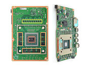
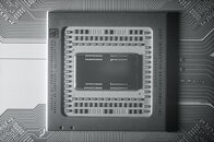
When AMD and Sony collaborated on making the next generation console chip, AMD has internally codenamed it Flute, while Sony codenamed it Oberon or Ariel. This PlayStation 5 SoC die has today been pictured thanks to the Fritzchens Fritz and we get to see a closer look at the die internals. Featuring eight of AMD's Zen2 cores that can reach frequencies of up to 3.5 GHz, the CPU is paired with 36 CU GPU based on the RDNA 2 technology. The GPU is capable of running at speed of up to 2.23 GHz. The SoC has been made to accommodate all of that hardware, and bring IO to connect it all.

When tearing down the console, the heatsink and the SoC are connected by liquid metal, which is used to achieve the best possible heat transfer between two surfaces. Surrounding the die there is a small amount of material used to prevent liquid metal (a conductive material) from possibly spilling and shorting some components. Using a special short wave infrared light (SWIR) microscope, we can take a look at what is happening under the hood without destroying the chip. And really, there are a few distinct areas that are highlighted by the Twitter user @Locuza. As you can see, the die has special sectors with the CPU complex and a GPU matrix with plenty of workgroups and additional components for raytracing.

AMD Talks Zen 4 and RDNA 3, Promises to Offer Extremely Competitive Products

AMD is always in development mode and just when they launch a new product, the company is always gearing up for the next-generation of devices. Just a few months ago, back in November, AMD has launched its Zen 3 core, and today we get to hear about the next steps that the company is taking to stay competitive and grow its product portfolio. In the AnandTech interview with Dr. Lisa Su, and The Street interview with Rick Bergman, the EVP of AMD's Computing and Graphics Business Group, we have gathered information about AMD's plans for Zen 4 core development and RDNA 3 performance target.

Starting with Zen 4, AMD plans to migrate to the AM5 platform, bringing the new DDR5 and USB 4.0 protocols. The current aim of Zen 4 is to be extremely competitive among competing products and to bring many IPC improvements. Just like Zen 3 used many small advances in cache structures, branch prediction, and pipelines, Zen 4 is aiming to achieve a similar thing with its debut. The state of x86 architecture offers little room for improvement, however, when the advancement is done in many places it adds up quite well, as we could see with 19% IPC improvement of Zen 3 over the previous generation Zen 2 core. As the new core will use TSMC's advanced 5 nm process, there is a possibility to have even more cores found inside CCX/CCD complexes. We are expecting to see Zen 4 sometime close to the end of 2021.

AMD Ryzen 5000 Cezanne APU Die Render Leaked

VideoCardz has recently received a render of the upcoming AMD Ryzen 5000 Cezanne APU which is expected to be unveiled next week. The Zen 3 Cezanne APUs support up to 8 cores and 16 threads just like Zen 2 Renoir APUs. The Cezanne APU should support up to 8 graphics cores and 20 PCIe lanes, it is currently unknown whether these lanes will be PCIe 3.0 or PCIe 4.0. The Cezanne die appears to be ~10% larger than Renoir which comes from the larger Zen 3 core design and a larger L3 cache of 16 MB. The new Ryzen 5000H Cezanne series processors are expected to be announced by AMD next week and will power upcoming low and high power laptops.

AMD Ryzen 5 5600H "Cezanne" Processor Benchmarked, Crushes Renoir in Single Core and Multi Core Performance

With the launch of AMD's next-generation mobile processors just around the corner, with an expected launch date in the beginning of 2021 at the CES virtual event. The Cezanne lineup, as it is called, is based on AMD's latest Zen 3 core, which brings many IPC improvements, along with better frequency scaling thanks to the refined architecture design. Today, we get to see just how much the new Cezanne generation brings to the table thanks to the GeekBench 5 submission. In the test system, a Ryzen 5 5600H mobile processor was used, found inside of a Xiaomi Mi Notebook, paired with 16 GB of RAM.

As a reminder, the AMD Ryzen 5 5600H is a six-core, twelve threaded processor. So you are wondering how the performance looks like. Well, in the single-core test, the Zen 3 enabled core has scored 1372 points, while the multi-threaded performance result equaled 5713 points. If we compare that to the last generation Zen 2 based "Renoir" design, the equivalent Ryzen 5 4600H processor, the new design is about 37% faster in single-threaded, and about 14% faster in multi-threaded workloads. We are waiting for the announcement to see the complete AMD Cezanne lineup and see the designs it will bring.

The Ultimate Zen: AMD's Zen 3 Achieves 89% Higher Performance Than First-generation Zen

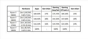
An investigative, generation-upon-generation review from golem.de paints an extremely impressive picture for AMD's efforts in iterating upon their original Zen architecture. While the first generation Zen achieved a sorely needed inflection point in the red team's efforts against arch-rival Intel and its stranglehold in the high-performance CPU market, AMD couldn't lose its vision on generational performance improvements on pain of being steamrolled (pun intended) by the blue giant's sheer scale and engineering prowess. However, perhaps this is one of those showcases of "small is nimble", and we're now watching Intel slowly changing its posture, crushed under its own weight, so as to offer actual competition to AMD's latest iteration of the Zen microarchitecture.

The golem.de review compares AMD's Zen, Zen+, Zen 2 and Zen 3 architectures, represented by the Ryzen 7 1800X, Ryzen 7 2700X, Ryzen 7 3800X and Ryzen 7 5800X CPUs. Through it, we see a generational performance increase that mostly exceeds the 20% performance points across every iteration of Zen when it comes to both gaming and general computing workloads. This generational improvement hits its (nowadays) most expressive result in that AMD's Ryzen 7 5800X manages to deliver 89% higher general computing, and 84% higher gaming performance than the company's Zen-based Ryzen 7 1800X. And this, of course, ignoring performance/watt improvements that turn the blue giant green with envy.

GIGABYTE Unveils AMD Ryzen Threadripper Pro Motherboard for Servers

AMD Ryzen Threadripper Pro line of HEDT/Workstation processors were a nothingburger for the DIY PC crowd as it was launched exclusively through Lenovo for its ThinkStation P620 line of workstations. These processors are a step-up from the retail Threadripper 3000 series, as they feature the full 8-channel DDR4 memory interface, and 128 PCI-Express Gen 4 lanes of the "Zen 2" based "Rome" MCM. The retail Threadripper 3000 chips only feature a quad-channel (4-channel) memory interface.

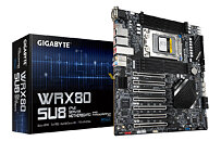
GIGABYTE has developed a custom server motherboard based on the AMD WRX80 chipset that drives the Lenovo ThinkStation P620. The new WRX80 SU8 motherboard by GIGABYTE features a single sWRX8 CPU socket, supporting Threadripper Pro processors up to the Threadripper Pro 3995WX. It features seven PCI-Express 4.0 x16 slots, three 64 Gbps U.2 ports, two M.2-22110 slots, and eight DDR4 DIMM slots, each with its own dedicated memory channel. GIGABYTE also used the lavish PCIe budget of this platform to give the board dual 10 GbE interfaces. The board also comes with an ASPEED IPMI remote management chip. GIGABYTE is a server vendor, and this board's unveiling could hint at the likelihood of AMD opening up availability of the Threadripper Pro to other OEM vendors, ending Lenovo's exclusivity.

Cyberpunk 2077 System Requirements Lists Updated, Raytracing Unsupported on RX 6800 Series at Launch

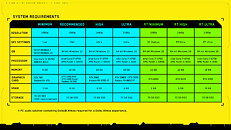
CD Projekt RED released updated PC system requirements lists for "Cyberpunk 2077," which will hopefully release before the year 2077. There are a total of seven user experience grades, split into conventional raster 3D graphics, and with raytracing enabled. The bare minimum calls for at least a GeForce GTX 780 or Radeon RX 480; 8 GB of RAM, Core i3 "Sandy Bridge" or AMD FX "Bulldozer," and 64-bit Windows 7. The 1080 High grade needs at least a Core i7 "Haswell" or Ryzen 3 "Raven Ridge" processor, 12 GB of RAM, GTX 1060 6 GB or GTX 1660 Super or RX 590 graphics. The 1440p Ultra grade needs the same CPUs as 1080p High, but with steeper GPU requirements of at least an RTX 2060 or RX 5700 XT.

The highest sans-RT grade, 4K UHD Ultra, needs either the fastest i7-4790 "Haswell" or Ryzen 5 "Zen 2" processor, RTX 2080 Super or RTX 3070, or Radeon RX 6800 graphics. Things get interesting with the three lists for raytraced experience. 1080p Medium raytraced needs at least an RTX 2060; 1440p High raytraced needs an RTX 3070, and 4K UHD Ultra raytraced needs at least a Core i7 "Skylake" or Ryzen 5 "Zen 2" chip, and RTX 3080 graphics. All three raytraced presets need 16 GB of RAM. Storage requirements across the board are 70 GB, and CDPR recommends the use of an SSD. What's interesting here is that neither the RX 6800 nor RX 6800 XT make it to the raytraced list (despite the RX 6800 finding mention in the non-raytraced lists). PC Gamer reports that Cyberpunk 2077 will not enable raytracing on Radeon RX 6800 series at launch. CDPR, however, confirmed that it is working with AMD to optimize the game for RDNA2, and should enable raytracing "soon."

AMD Unveils Ryzen Embedded V2000 Processors with Enhanced Performance and Efficiency

AMD today launched a new product in its high-performance Embedded processor family, the AMD Ryzen Embedded V2000 Series processor. Built on the innovative 7 nm process technology, "Zen 2" cores and high-performance AMD Radeon graphics, the AMD Ryzen Embedded V2000 Series provides a new class of performance with 7 nm technology, incredible power efficiency and continues to deliver enterprise-class security features for embedded customers.

The AMD Embedded Ryzen V2000 family is designed for embedded applications such as Thin Client, MiniPC and Edge systems. Equipped with up to eight CPU cores and seven GPU compute units, a single AMD Ryzen Embedded V2000 Series processor provides 2x the multi-threaded performance-per-watt, up to 30 percent better single-thread CPU performance and up to 40 percent better graphics performance over the previous generation. For customers and applications that need high-performance display capabilities, the Ryzen Embedded V2000 series can power up to four independent displays in 4K resolution.

AMD "Lucienne" Silicon to Power Certain Ryzen 5000 Series APUs

There's been much chatter in the social media about a new piece of AMD APU silicon, codenamed "Lucienne." It's being rumored that "Lucienne" is a refresh of the current-generation "Renoir" silicon, and is an APU with eight "Zen 2" CPU cores and eight "Vega" NGCUs. One of the first SKUs based on the die is the Ryzen 7 5700U, which surfaced on the AoTS benchmark database.

The 5700U is possibly a 15 W ultra-portable processor, and according to the AoTS benchmark screenshot, it comes with an 8-core/16-thread CPU (the 4700U is 8-core/8-thread). The addition of SMT helps the 5700U shore up much of its performance lead over the 4700U. It also turns out that the Ryzen 5000 will see two APU dies driving AMD's product-stack, with "Lucienne" powering the Ryzen 5 5500U and Ryzen 7 5700U; while the newer "Cezanne" die, which introduces "Zen 3" CPU cores, powers the Ryzen 5 5600U and the Ryzen 7 5800U.

Intel 14 nm Node Compared to TSMC's 7 nm Node Using Scanning Electron Microscope

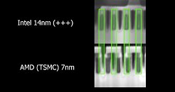
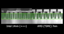
Currently, Intel's best silicon manufacturing process available to desktop users is their 14 nm node, specifically the 14 nm+++ variant, which features several enhancements so it can achieve a higher frequencies and allow for faster gate switching. Compare that to AMD's best, a Ryzen 3000 series processor based on Zen 2 architecture, which is built on TSMC's 7 nm node, and you would think AMD is in clear advantage there. Well, it only sort of is. German hardware overclocker and hacker, der8auer, has decided to see how one production level silicon compares to another, and he put it to the test. He decided to use Intel's Core i9-10900K processor and compare it to AMD's Ryzen 9 3950X under a scanning electron microscope (SEM).

First, der8auer took both chips and detached them from their packages; then he proceeded to grind them as much as possible so SEM could do its job of imaging the chips sans the substrate and protective barrier. This was followed by securing the chips to a sample holder using an electrically conductive adhesive to improve penetration of the high energy electrons from the SEM electron gun. To get as fair a comparison as possible, he used the L2 cache component of both processors as they are usually the best representatives of a node. This happens because the logic portion of the chip differs according to architecture; hence, level two cache is used to get a fair comparison - it's design is much more standardized.

ClockTuner for Ryzen Simplifies "Zen 2" Overclocking, Squeezes Out Double-digit Percent Performance

ClockTuner for Ryzen (CTR) by Yuri "1usmus" Bubliy, is an evolution of the DRAM Calculator for Ryzen utility. The utility goes beyond the functionality of the DRAM Calculator - which finds the most precise memory settings for Ryzen processors - and does your homework for Ryzen CPU overclocking. Optimized for processors based on the "Zen 2" microarchitecture, CTR has been designed both for Socket AM4 and sTRX4 (Threadripper) processors, and Linus Tech Tips in its announcement video of CTR demonstrated the tool's prowess in squeezing out a neat 10% performance gain for their Threadripper 3960X processor. Besides CPU and memory settings, the tool performs stability testing and benchmarking. 1usmus expects to release CTR 1.0 in September 2020.

AMD Warhol, Van Gogh, and Cezanne to Make Up Company's 5th Gen Ryzen

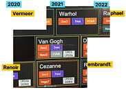
A May 2020 report put together with info from multiple sources pointed towards AMD's client-segment product roadmap going as far into the future as 2022. The roadmap was partial, with a few missing bits. VideoCardz attempted to reconstruct the roadmap based on new information from one of the primary sources of the May leak, @MeibuW. According to the roadmap, 2020 will see AMD debut its 4th Gen Ryzen "Vermeer" desktop processors featuring "Zen 3" CPU cores, built on TSMC N7e or N7P silicon fabrication process, and offering PCIe Gen 4. The "Renoir" APU silicon combining up to 8 "Zen 2" CPU cores with a 512-SP "Vega" iGPU debuted on the mobile platform, and recently launched on the desktop platform as an OEM-exclusive. It remains to be seen if AMD launches this in the DIY retail channel.

2021 is when three new codenames from AMD get some air-time. "Warhol" is codename for the 5th Gen Ryzen part that succeeds "Vermeer." Interestingly, it too is shown as a combination of "Zen 3" CPU cores, PCIe Gen 4, and 7 nm. Perhaps AMD could innovate in areas such as DRAM (switch to PC DDR5), and maybe increase core counts. DDR5 could herald a new socket, after 4 years of AM4. The second silicon bound for 2021 is "Van Gogh," an APU that combines "Zen 2" CPU cores with an RDNA2 iGPU. Interestingly, "Cezanne," bound for the same year, has the opposite CPU+iGPU combination - a newer gen "Zen 3" CPU component, and an older gen "Vega" iGPU. The two chips could target different markets, looking at their I/O, with "Van Gogh" supporting LPDDR5 memory.

Microsoft Details Xbox Series X SoC, Drops More Details on RDNA2 Architecture and Zen 2 CPU Enhancements

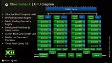
Microsoft in its Hot Chips 32 presentation detailed the SoC at the heart of the upcoming Xbox Series X entertainment system. The chip mostly uses AMD IP blocks, and is built on TSMC N7e (enhanced 7 nm) process. It is a 360.4 mm² die with a transistor count of 15.3 billion. Microsoft spoke about the nuts and bolts of the SoC, including its largest component - the GPU based on AMD's new RDNA2 graphics architecture. The GPU takes up much of the chip's die area, and has a raw SIMD throughput of 12 TFLOP/s. It meets DirectX 12 Ultimate logo requirements, supporting hardware-accelerated ray-tracing.

The RDNA2 GPU powering the Xbox Series X SoC features 52 compute units spread across 26 RDNA2 dual compute units. The silicon itself physically features two additional dual CUs (taking the total physical CU count to 56), but are disabled (possibly harvesting headroom). We've detailed first-generation RDNA architecture in the "architecture" pages of our first AMD Radeon RX 5000-series "Navi" graphics card reviews, which explains much of the SIMD-level innovations from AMD that help it drive a massive SIMD IPC gain over the previous-generation GCN architecture. This hierarchy is largely carried over to RDNA2, but with the addition of a few SIMD-level components.

NUVIA Phoenix SoC is 40-50 Percent Faster Than Zen 2 for a Third of Power

Last year, in November of 2019, a startup company called NUVIA Inc. broke out of the stealth mode and decided to reveal itself to the public. Focused on "re-imagining silicon", the company is led by some of the brightest minds in the semiconductor industry. Some people like Gerard Williams III, the CEO of the company, previously served as a chief CPU architect at Apple and has spent over 10 years at Arm before that. Others like Manu Gulati and John Bruno serve as senior vice presidents of silicon and system engineering respectively. Together, their people are forming a company full of well-known industry names. Of course, there are more and you should check out this page.

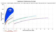
NUVIA Inc. promises to deliver only the best performance and "re-imagine silicon" as they say. Today, we got some bold claims from the company regarding the performance of their upcoming Phoenix SoC. Using Geekbench 5, the company has provided some simulated results of how the Phoenix SoC will perform. Being that it runs on Arm ISA, the SoC can run at very low power and achieve good performance. NUVIA has run some simulations and it expects its Phoenix SoC to be 40-50% faster in single-threaded performance than Zen 2/Sunny Cove at just a third of the power, 33% of the percent of power to be precise. In the graph below, NUVIA has placed its SoC only in 5 W range, however, the company said that they have left the upper curve to be disclosed at later date, meaning that the SoC will likely compete in high-performance markets and at higher power targets. While these claims are to be taken with a grain of salt, it is now a waiting game to see how NUVIA realizes its plans.
NUVIA Inc. Logo NUVIA Phoenix SoC Performance
Return to Keyword Browsing
Jan 10th, 2025 12:48 EST change timezone

New Forum Posts

Popular Reviews

Controversial News Posts