Wednesday, December 21st 2011

Cost-Effective Radeon HD 7900 PCB Already In The Works
A little earlier today, we showed you pictures of AMD's first Radeon HD 7900 series single-GPU PCB that makes use of digital-PWM power delivery. Some of the first batches of Radeon HD 7900 graphics cards will stick to that PCB and board design, as it's backed by AMD's engineering. Even as the SKU's launch is less than 24 hours away, there are pictures of AMD's cost-effective Radeon HD 7900 PCB surfacing on Asian media sites. Once ready, AMD add-in board partners can opt for this cost-effective PCB if they want to fine-tune their prices. It looks like AMD is ready well ahead to face competition from NVIDIA, with its GeForce Kepler 104 (GK104) GPU.
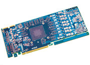
The cost-effective PCB, without any components laid, is pictured below. The first picture shows its obverse side, the second, its reverse side. The PCB is completely up to speed with everything Tahiti GPU will need. It has provision for two 8-pin PCIe power inputs, an 8+2 phase cost-effective analog VRM, probably driven by a cost-effective CHIL controller, and a different display output connector loadout. It has provision for two DVI, and one each of HDMI and full-size DisplayPort. Partners can still use a single DVI connector, and keep their cards single-slot capable. Provisions for 12 GDDR5 chips are right where they should be. There is nothing eventful in the reverse side, just traces for all the supportive components.
Sources:
Weibo.com, Expreview
The cost-effective PCB, without any components laid, is pictured below. The first picture shows its obverse side, the second, its reverse side. The PCB is completely up to speed with everything Tahiti GPU will need. It has provision for two 8-pin PCIe power inputs, an 8+2 phase cost-effective analog VRM, probably driven by a cost-effective CHIL controller, and a different display output connector loadout. It has provision for two DVI, and one each of HDMI and full-size DisplayPort. Partners can still use a single DVI connector, and keep their cards single-slot capable. Provisions for 12 GDDR5 chips are right where they should be. There is nothing eventful in the reverse side, just traces for all the supportive components.


29 Comments on Cost-Effective Radeon HD 7900 PCB Already In The Works
Although, I ask is Nvidia intending to move what's known as "mainstream" and ramp pricing up to be in the league of "enthusiast"? What would they use to backfill between what's now a pedestrian GTX550 and this new a GK104? I suppose they just use the same approach as "non-ti" employed presently, (geldings' from GK104 production) as they've already grasped the proposition they’ll get extensive binning from TSMC on the GK104.
Also lot of folks who provide/dicussed the information to those specs', haven't reformulated what that mean's now with synchronous geometry. Will just boosting core clock and and extra cores be enough?
www.techpowerup.com/157039/NVIDIA-Kepler-To-Do-Away-with-Hotclocks.html