Monday, November 12th 2012

Haswell-ULT Processors Could Use 24 MHz BClk, New C-States, and MCM to Cut Power Draw
Going into 2013, Intel's tough balancing act between keeping a low power/thermal envelope, and advancing performance, all while staying on the 22 nm silicon fab process, will be care of its Core "Haswell-ULT" processor. The chip will feature some radical changes to traditional Intel processor design, which will help it achieve its design goals. According to a deck of leaked slides scored by Expreview, Intel plans to use additional C-states that drop the processor's base clock, and redesign the processor package to accommodate the PCH silicon, reducing the board footprint.
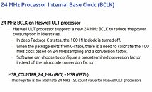
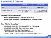
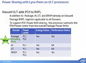
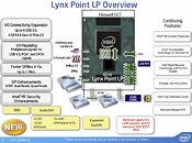
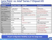
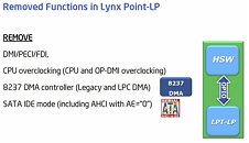
To begin with, Haswell-ULT will be designed to support 24 MHz base clock speed, which running in "deep" energy-saving idle states. Modern processors with FSB replacement interconnect technologies such as QuickPath Interconnect and HyperTransport need a base clock to time other components on the processor, and for low-level communications, while a bulk of the data is transported by the primary interconnect. Intel found a way to turn off the 100 MHz base clock signal (which is also used to time the PCI-Express root complex and integrated graphics core), and replace it with a 24 MHz clock, when the processor is idling. As the processor returns to lower (more active) C-states, the 100 MHz base clock is reapplied. The 24 MHz base clock is activated by three new power states, C8, C9, and C10, introduced by Haswell-ULT. The third slide below details what happens to the various components in the new C-states.Another major change, which is a step towards building a true high-performance SoC, is the Haswell-ULT package. The package is a multi-chip module (MCM) of the processor die and the PCH (platform-controller hub, or the chipset). One shouldn't confuse this with Core "Clarkdale" processors, which were MCMs of a dual-core CPU silicon, and a GMCH (graphics memory controller hub). The CPU silicon of Haswell-ULT includes up to four x86 cores, three levels of cache, integrated memory controller, integrated graphics, and a PCI-Express root complex. The PCH silicon includes all platform interfaces, including SATA, USB, SMBus, gigabit Ethernet, and HD audio. Think of PCH as being a glorified southbridge.The pin-side of the Haswell-ULT package, we imagine, features only I/O and power pins, with no chipset bus. The processor and PCH dies on the package are connected by what Intel is referring to as "OPI x8," which appears to feature double the bandwidth as DMI 2.0, that's 8 GB/s. The PCH that will drive Intel's Core "Haswell" processors across the board is codenamed "Lynx Point," which will exist as dedicated PCH packages on desktop and mainstream mobile platforms, and part of the Haswell-ULT MCMs, as Lynx Point-LP, with a slightly slimmer feature-set.
Source:
Expreview
To begin with, Haswell-ULT will be designed to support 24 MHz base clock speed, which running in "deep" energy-saving idle states. Modern processors with FSB replacement interconnect technologies such as QuickPath Interconnect and HyperTransport need a base clock to time other components on the processor, and for low-level communications, while a bulk of the data is transported by the primary interconnect. Intel found a way to turn off the 100 MHz base clock signal (which is also used to time the PCI-Express root complex and integrated graphics core), and replace it with a 24 MHz clock, when the processor is idling. As the processor returns to lower (more active) C-states, the 100 MHz base clock is reapplied. The 24 MHz base clock is activated by three new power states, C8, C9, and C10, introduced by Haswell-ULT. The third slide below details what happens to the various components in the new C-states.Another major change, which is a step towards building a true high-performance SoC, is the Haswell-ULT package. The package is a multi-chip module (MCM) of the processor die and the PCH (platform-controller hub, or the chipset). One shouldn't confuse this with Core "Clarkdale" processors, which were MCMs of a dual-core CPU silicon, and a GMCH (graphics memory controller hub). The CPU silicon of Haswell-ULT includes up to four x86 cores, three levels of cache, integrated memory controller, integrated graphics, and a PCI-Express root complex. The PCH silicon includes all platform interfaces, including SATA, USB, SMBus, gigabit Ethernet, and HD audio. Think of PCH as being a glorified southbridge.The pin-side of the Haswell-ULT package, we imagine, features only I/O and power pins, with no chipset bus. The processor and PCH dies on the package are connected by what Intel is referring to as "OPI x8," which appears to feature double the bandwidth as DMI 2.0, that's 8 GB/s. The PCH that will drive Intel's Core "Haswell" processors across the board is codenamed "Lynx Point," which will exist as dedicated PCH packages on desktop and mainstream mobile platforms, and part of the Haswell-ULT MCMs, as Lynx Point-LP, with a slightly slimmer feature-set.

13 Comments on Haswell-ULT Processors Could Use 24 MHz BClk, New C-States, and MCM to Cut Power Draw
Where does it leave the average enthusiast, again?
Lets hope we get more details soon.......please, Intel??
:wtf::roll:
- DEC alpha is one.
- Cray interconnects
And there video chips where also owned by another company thus why they can't make decent drivers for them. real 3d i think ...
ULT would have an onboard PCH known as the Lynx Point-LP which is thoroughly detailed in the article.
The notebook and desktop Haswell CPUs come with new overclocking features, slides from legitreviewsbelow:
I could see boards going like a hybrid m-itx/atx the length of ATX for the slots and the narrowness of m-itx with no south bridge etc.
L=12 x W=6.7
Though they would need to be wide enough for 4 RAM slots.
The reason the original Athlon was so awesome (and such a leap up from the K6-III) was Alpha-style design and technology that Dirk brought over when Jerry recruited him away from DEC. EV6 DDR FSB, x86 to RISC op (ROP) translation, multi-issue FPU, etc.