Tuesday, September 20th 2016

AMD Vega 10, Vega 20, and Vega 11 GPUs Detailed
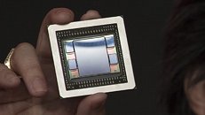
AMD CTO, speaking at an investors event organized by Deutsche Bank, recently announced that the company's next-generation "Vega" GPUs, its first high-end parts in close to two years, will be launched in the first half of 2017. AMD is said to have made significant performance/Watt refinements with Vega, over its current "Polaris" architecture. VideoCardz posted probable specs of three parts based on the architecture.
AMD will begin the "Vega" architecture lineup with the Vega 10, an upper-performance segment part designed to disrupt NVIDIA's high-end lineup, with a performance positioning somewhere between the GP104 and GP102. This chip is expected to be endowed with 4,096 stream processors, with up to 24 TFLOP/s 16-bit (half-precision) floating point performance. It will feature 8-16 GB of HBM2 memory with up to 512 GB/s memory bandwidth. AMD is looking at typical board power (TBP) ratings around 225W.Next up, is "Vega 20." This is one part we've never heard of today, and it's likely scheduled for much later. "Vega 20" is a die-shrink of Vega 10 to the 7 nm GF9 process being developed by GlobalFoundries. It will feature 4,096 stream processors, too, but likely at higher clocks, up to 32 GB of HBM2 memory running full-cylinders at 1 TB/s, PCI-Express gen 4.0 bus support, and a typical board power of 150W.
The "Vega 11" part is a mid-range chip designed to replace "Polaris 10" from the product-stack, and offer slightly higher performance at vastly better performance/Watt. AMD is expecting to roll out the "Navi" architecture some time in 2019, and so AMD will hold out for the next two years with "Vega." There's even talk of a dual-GPU "Vega" product featuring a pair of Vega 10 ASICs.
Source:
VideoCardz
AMD will begin the "Vega" architecture lineup with the Vega 10, an upper-performance segment part designed to disrupt NVIDIA's high-end lineup, with a performance positioning somewhere between the GP104 and GP102. This chip is expected to be endowed with 4,096 stream processors, with up to 24 TFLOP/s 16-bit (half-precision) floating point performance. It will feature 8-16 GB of HBM2 memory with up to 512 GB/s memory bandwidth. AMD is looking at typical board power (TBP) ratings around 225W.Next up, is "Vega 20." This is one part we've never heard of today, and it's likely scheduled for much later. "Vega 20" is a die-shrink of Vega 10 to the 7 nm GF9 process being developed by GlobalFoundries. It will feature 4,096 stream processors, too, but likely at higher clocks, up to 32 GB of HBM2 memory running full-cylinders at 1 TB/s, PCI-Express gen 4.0 bus support, and a typical board power of 150W.
The "Vega 11" part is a mid-range chip designed to replace "Polaris 10" from the product-stack, and offer slightly higher performance at vastly better performance/Watt. AMD is expecting to roll out the "Navi" architecture some time in 2019, and so AMD will hold out for the next two years with "Vega." There's even talk of a dual-GPU "Vega" product featuring a pair of Vega 10 ASICs.

194 Comments on AMD Vega 10, Vega 20, and Vega 11 GPUs Detailed
Edit: Don't confuse HBM2 to better then HBM in general. It's still the same clocks and bandwidth compared to HBM. The only difference is is the stacking of chips which makes it up to 16GB of HBM2 memory. Perhaps even more.
( P.S. You might want to check FuryX's & RX480's pathetic performance at VR benchmarks. www.hardocp.com/reviews/vr/
So much again for Raja's hype about "premium VR performance" !!)
www.guru3d.com/news-story/amd-vega-10-vega-20-and-vega-11-gpus-mentioned-by-cto.html
They said that the article is still being rewritten but they seem to be the only one to make that statement.
(Probably you didn't even bother to check the link i put because your thoughts are pure red!;) )
Next time i'll ask for your approval before i post a link. You seem to be an objective person after all.
Smaller interposer, reduced cost, and many knock-on benefits from this.
Some models MAY have four stacks (16GB, IIRC, would actually require that), but I don't think we need more than 8GB for consumer cards for the next couple of years - even at the high end. We have yet to see 8GB be stressed... it's sometimes hard enough just to max out 4GB.
It is updated from GCN4 (which is already 15% faster than the GCN in Fury X), has all of the updated geometry engines, schedulers, etc... of Polaris - all updated yet another generation. It is using the second generation HBM memory, with double the bandwidth of RX 480 (but only 77% more shaders to feed).
So, at WORST, Vega 10 is Fury X + 15% + 15% + 15% = ~50% faster than Fury X.
That is to say:
~15% higher IPC
~15% boost from clock speed
~15% boost from bandwidth
And that's just assuming a scaled-up Polaris GPU... which Vega 10 is not.
Still, maybe only add 10% for architectural improvements after Polaris - Vega only has another six months of development on it compared to Polaris... but that's 67% faster than Fury X...
Everything after that has been pretty underwhelming for me
Regardless of what the naysayers saying about the noise and heat, it was the best gpu release i've ever witnessed
cant speak much about the probability of it happening with the Vega release but one can hope at least :^(
I dont want to see x70 cards in the $500-700 range next time Nvidia releases something new again
:roll: :roll: :roll:
There are cases where code can actually pull 5.8 TFLOPS effective out of RX480, but that happens rarely even for gpgpu compute devs let alone gamers :laugh:Bingo. We had a little discussion about it here on TPU: www.techpowerup.com/forums/threads/maxwell-and-pascal-secretly-use-tile-based-rasterization.224773/
Their tile based rendering isn't completely "tile based", only the rasterization part ... they keep the tile size small enough so it can fit completely into first level cache ... all for a magical efficiency increase
VR performance? Hand in the air if you really care about VR performance right now. Worried that tech demo run will not be smooth?? VR is a niche, that is all. Let's move on.
Fury X was showing lackluster performance and meh overclockability when it was just released.
TODAY Fury X is showing its true power and there is actually a lot more still in the can (stock cooled Fury X throttles) - it is still competing against top end GPUs like 980ti (comfortably beating it at 4K, and equal or better in almost any DX12/Vulkan game, 2-3% lower in DX11 lower res), 1070 and in an edge case, the 1080. So let's turn this around: AMD's ONLY HBM offering in last years' (!) line up is now competing with Nvidia's most shiny new arch. The entire rest of AMDs line up, including the RX480, is getting swamped with a lower amount of shaders from the competition.
And there you are, saying HBM is junk and not of use for GPUs. Mkay :)
Also, a general note and to unburden our kind mods... STOP DOUBLE POSTING AND USE AN EDIT BUTTON