Tuesday, September 20th 2016

AMD Vega 10, Vega 20, and Vega 11 GPUs Detailed
AMD CTO, speaking at an investors event organized by Deutsche Bank, recently announced that the company's next-generation "Vega" GPUs, its first high-end parts in close to two years, will be launched in the first half of 2017. AMD is said to have made significant performance/Watt refinements with Vega, over its current "Polaris" architecture. VideoCardz posted probable specs of three parts based on the architecture.
AMD will begin the "Vega" architecture lineup with the Vega 10, an upper-performance segment part designed to disrupt NVIDIA's high-end lineup, with a performance positioning somewhere between the GP104 and GP102. This chip is expected to be endowed with 4,096 stream processors, with up to 24 TFLOP/s 16-bit (half-precision) floating point performance. It will feature 8-16 GB of HBM2 memory with up to 512 GB/s memory bandwidth. AMD is looking at typical board power (TBP) ratings around 225W.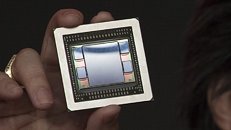 Next up, is "Vega 20." This is one part we've never heard of today, and it's likely scheduled for much later. "Vega 20" is a die-shrink of Vega 10 to the 7 nm GF9 process being developed by GlobalFoundries. It will feature 4,096 stream processors, too, but likely at higher clocks, up to 32 GB of HBM2 memory running full-cylinders at 1 TB/s, PCI-Express gen 4.0 bus support, and a typical board power of 150W.
The "Vega 11" part is a mid-range chip designed to replace "Polaris 10" from the product-stack, and offer slightly higher performance at vastly better performance/Watt. AMD is expecting to roll out the "Navi" architecture some time in 2019, and so AMD will hold out for the next two years with "Vega." There's even talk of a dual-GPU "Vega" product featuring a pair of Vega 10 ASICs.
Source:
VideoCardz
AMD will begin the "Vega" architecture lineup with the Vega 10, an upper-performance segment part designed to disrupt NVIDIA's high-end lineup, with a performance positioning somewhere between the GP104 and GP102. This chip is expected to be endowed with 4,096 stream processors, with up to 24 TFLOP/s 16-bit (half-precision) floating point performance. It will feature 8-16 GB of HBM2 memory with up to 512 GB/s memory bandwidth. AMD is looking at typical board power (TBP) ratings around 225W.

The "Vega 11" part is a mid-range chip designed to replace "Polaris 10" from the product-stack, and offer slightly higher performance at vastly better performance/Watt. AMD is expecting to roll out the "Navi" architecture some time in 2019, and so AMD will hold out for the next two years with "Vega." There's even talk of a dual-GPU "Vega" product featuring a pair of Vega 10 ASICs.
194 Comments on AMD Vega 10, Vega 20, and Vega 11 GPUs Detailed
www.techpowerup.com/reviews/NVIDIA/GeForce_GTX_1070/24.html
They are roughly equal, and that isn't even including the new games like Deus Ex.
As for "all hope is lost". I think people need to realize that (at least for now) it seems like AMD'S current strategy is working. Marketshare is far more important to AMD than a halo product right now. Also anyone remember the days when RADEON had 40-52% marketshare and was profiting like crazy? Well that was back in the 4000/5000/6000 Era when they werent trying to win a absolute performance. I loved the 7970/290X, but apparently it didn't make AMD much money... :/
On a different note Nvidia did rebrand years ago because they were selling cards better than amd and still does but refresh now but amd has been doing that more than nvidia has recently and are doing worst in graphics sales.
The 780 and 280X are on it buddy...
Deep learning/neural networks can use half precision...
Gaming doesn't have a 1:1 correlation with Tflops anyways so just go with the bigger number ;)
I see a bunch of others share my sentiments, good thing I held off on hitting 'post reply' LoLoLoLoL
Nvidia always threw a larger bus at inferior memory.
HD 4870 vs GTX 280 etc, GDDR5 on 256 vs GDDR3 on 512.
ATi 3K series with DDR4.
AMD showed us that with the Bulldozer arch... crap CPU but the idea was cool.
and RX480 with consistent R9 390x levels of performance at a lower power usage sounds like music to my ears.
And anything to bring the prices down of the higher segment is great :)
I still remember all the glorious comments from AMD about the use of HBM memory, and after months & months of hype and brainwash, this supreme card struggle to compete with a reference 980Ti (*and stayed far behind the aftermarket Ti s).
I've said it back then and i'll say it again. HBM technology was already known to the companies years ago. There was no chance a colossus company like NVidia not having done their own research with HBM. So in order not to use them (*back then at least), made me suspect that there were disadvantages at HBM's usage.
Indeed, the HBM memory was only limited to 4GB size, which led to the downfall of FuryX's effort for the top.
( Just like last time, there is no way that again NVidia not having made their own research for the HBM2.)
I do believe though that from a shareholder point of view, Vega HAS to perform well. I look forward to seeing it in action.
Maxwell and Pascal have this, and that's why they are so efficient and have such lower buses and yet perform on par or better with double bus on AMD side.
Tile based rendering was introduced by PowerVR back in 1996.
Read more:
www.anandtech.com/show/735/3
en.wikipedia.org/wiki/Tiled_rendering