Thursday, January 12th 2017

AMD's Vega-based Cards to Reportedly Launch in May 2017 - Leak
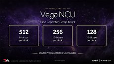
According to WCCFTech, AMD's next-generation Vega architecture of graphics cards will see its launch on consumer graphics solutions by May 2017. The website claims AMD will have Vega GPUs available in several SKUs, based on at least two different chips: Vega 10, the high-end part with apparently stupendous performance, and a lower-performance part, Vega 11, which is expected to succeed Polaris 10 in AMD's product-stack, offering slightly higher performance at vastly better performance/Watt. WCCFTech also point out that AMD may also show a dual-chip Vega 10×2 based card at the event, though they say it may only be available at a later date.AMD is expected to begin the "Vega" architecture lineup with the Vega 10, an upper-performance segment part designed to disrupt NVIDIA's high-end lineup, with a performance positioning somewhere between the GP104 and GP102. This chip should carry 4,096 stream processors, with up to 24 TFLOP/s 16-bit (half-precision) floating point performance. It will feature 8-16 GB of HBM2 memory with up to 512 GB/s memory bandwidth. AMD is looking at typical board power (TBP) ratings around 225W.
Next up, is "Vega 20", which is expected to be a die-shrink of Vega 10 to the 7 nm GF9 process being developed by GlobalFoundries. It will supposedly feature the same 4,096 stream processors, but likely at higher clocks, up to 32 GB of HBM2 memory at 1 TB/s, PCI-Express gen 4.0 bus support, and a typical board power of 150W.
AMD plans to roll out the "Navi" architecture some time in 2019, which means the company will use Vega as their graphics architecture for two years. There's even talk of a dual-GPU "Vega" product featuring a pair of Vega 10 ASICs.
Source:
WCCFTech
Next up, is "Vega 20", which is expected to be a die-shrink of Vega 10 to the 7 nm GF9 process being developed by GlobalFoundries. It will supposedly feature the same 4,096 stream processors, but likely at higher clocks, up to 32 GB of HBM2 memory at 1 TB/s, PCI-Express gen 4.0 bus support, and a typical board power of 150W.
AMD plans to roll out the "Navi" architecture some time in 2019, which means the company will use Vega as their graphics architecture for two years. There's even talk of a dual-GPU "Vega" product featuring a pair of Vega 10 ASICs.


187 Comments on AMD's Vega-based Cards to Reportedly Launch in May 2017 - Leak
But it's impossible for the GPU to do this itself, since it only sees memory accesses and instructions and clear patterns in these.
Performance is from the "Performance Summary" table in the Titan X Pascal review for 1440p. And I made the disclaimer that this methodology is super "hand-wavey".
Yeah, I get it. It's imperfect for many reasons and wrong for others. But it at least provides some sort of methodology for trying to make predictions.
If you think that a different methodology would be better, then put the info into a spreadsheet and show us what you come up with.
EDIT:
Once you plot everything out, it's pretty easy to see that those changes don't actually mean much for either company. The linear model actually fits pretty well over the past couple generations.
Personally, I think the biggest issue with this model is that the FuryX drastically skews the projection down for high FLOPs cards. If we set the intercepts to 0 (as makes logical sense) the picture changes a bit:
If you want to point out how this methodology is flawed/wrong/terrible, it would help to show us what you think is better. With pictures and stuff.
I.E. Titan X Gflops are given as 2*1.417GHz*3584cc=10,157GFlops while in gaming gpu clock is higher than that, in tpus review boost clock for titan xp is ~1.62GHz which means 2*1.62GHz*3584cc= 11,612GFlops. Why this matters is that real boost clock for nvidia's cards varies more per card and thus the real GFlops differs more from the given value.
I'm more interested in Vega 11. It a more mainstream product, and if it really does deliver good performance/watt (better than Pascal), that would be something. It would also give AMD a true laptop card.
The graphs & charts I made aren't 'wrong' or 'flawed'. They follow standard practices.
What you're doing--making specific modifications due to information you have--is more in line with Bayesian statistics.
It's not better, it's not worse. It's different.
......but in the mean time even after Amd's new power up Nvdia's like
Look at their product roadmap:
2015 = Fury HBM, R9 300 28nm
2016 = Polaris 10, 11
2017 = Vega 10, 11
Just read their bloody map!!! 2016 had the 480 as a stopgap while they got their nearly all HBM2 line-up ready.
HBM has so far been a bad move for AMD, and it's not going to help Vega 10 for gaming either. GP102 doesn't need it, and it's still going to beat Vega 10. HBM or better will be needed eventually, but let's see if even Volta needs it for gaming. AMD should have spent their resources on the GPU rather than memory bandwidth they don't need.
It's not likely though
(I'm assuming Vega 10 will beat Pascal in Perf/watt but not in throughput)