Wednesday, April 5th 2017

AMD's RX 580, 570 and RX 550 Specifications and 3D Mark Results Leak
So, it would appear that rumors and leaks about the RX 500 series being simple rebrands of AMD's RX 400 line were true. Recent leaks point to no more changes and performance increases than those achieved through higher base clock speeds on the graphics cards' GPU and memory. The architecture is the same, and the process seems to have followed the same path - as of yet, no confirmation regarding whether or not these cards do use a newer, leaner LPP process for higher clocks and less power consumption.
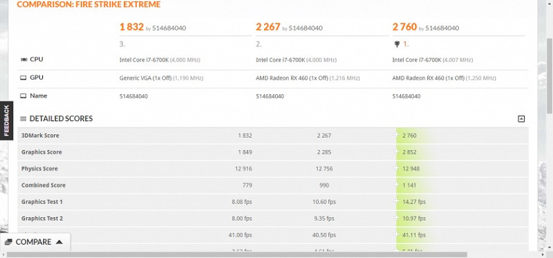
The RX 580 will come in with clocks at 1340 MHz with 4 GB and 8 GB GDDR5 variants clocking in at 8.0 GHz along a 256-bit bus interface. This amounts to 256 GB/s of bandwidth, and pricing should be around the $199 - $249 mark. On the leaked Firestrike Extreme test, this card was clocked to 1500 MHz (not easy to achieve with current Polaris 10 GPUs) and a 6675 points score. The RX 570, on the other hand, seems to have not been given the core clocks bump treatment, but memory speeds should see an increase to 7 GHz, delivering 224 GB/s of bandwidth. Overclocked to 1325 MHz, it delivered a score of 5719 points in the same benchmark. Finally, the new kid on the block, AMD's Polaris 12 is somewhat of a head-scratcher of a part, with its measly 640 stream processors (the line between discrete graphics and integrated ones is really blurry here). RX 550 reference cards should come in at 1190 MHz, where it scores 1849 in 3DMark FireStrike Extreme, though the card does so with only PCIe power.

 Pricing should be in line with AMD's RX 400 series, and performance should be comparable to RX 400 AIB cards, so no setting the world on fire here. If delay reports are true, expect these to be launched on April 18th. The RX 560 is MIA for now, but there is no reason to think it won't be launched alongside the other cards in the RX 500 line.
Sources:
WCCFTech, ETeknix


90 Comments on AMD's RX 580, 570 and RX 550 Specifications and 3D Mark Results Leak
P.S. 780 isn't 20% stronger than the pathetic 680 lol:
tpucdn.com/reviews/NVIDIA/GeForce_GTX_980/images/perfrel_1920.gif
If my memory serves me correctly, there were many rumor articles mentioning both. Although the more credible ones said LPE.
It is quite possible the 480 was made on dirt cheap 14nm LPE, and LPP was saved for the 500/Vega series. In fact that has been my hunch the entire time...
Sorry I was a couple % off.. :toast:
At most it will be a new silicon revision.
I mean what joke is this,laugh of us.
It's an odd pass time to meWhere's your rumour busting proof because afaik and most of the industry knew , when Polaris came out only Lpe was available LPP has not been available long ,afaik RyZen is AMD's first cut at LPP though there is no Lpe anymore so that's deffinately not used.
Lpe wasn't dirt cheap btw , at risk production never is but it will have been subsidized in all likelihood.
AMD usually holds the best Prices Performance crown. VEGA, based on what we've been told, will be the GPU game changer. Will be what Fury X was suppose to have been.
Since the VAST majority of PC gamers are going to top out at 1070ish pricing I would like to see AMD make their current offering more efficient. Would be nice to see 480 performance at 120 watts and lower temps, especially the VRMs. I think trying to revolutionize the CPU and GPU space at the same time when you have no money is going to be pretty hard. Polaris was just a sloppy release.
Would be curious to see 470 and 480 performance, temps and power usage with the cards running at 1100-1200.
Win7.I don't know about Win10.
wccftech.com/samsung-globalfoundries-tsmc-finfet-production/
It is a smart way to operate from a business perspective especially if you are AMD operating on tight budget with little room for error.
Intel, with piles of cash can afford failure. AMD cannot.
I only say Game Changer about VEGA because it looks very impressive. But I have a suspicion, in order to utilize VEGA to its fullest extent, it may need special specific programing. Because it's quite different from what's out today ATM.
Those that are familiar with programming and coding may have better in site.
On GPU side of things it is a 16nm TSMC (woot) 40 CU (480 is 36) GPU.
Very puzzled I am.
Actually on an interesting note: I think I read an article that dissected how Polaris had a bigger die than it needed to be, but that was likely to make it have good yields.
It really seems like AMD truly built Polaris to be an incredibly cheap-to-produce Mid-High End gaming family, and then Vega will be the densely packed enthusiast line.