Thursday, October 26th 2017

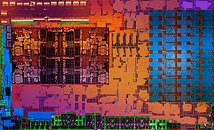
AMD "Raven Ridge" Silicon Detailed
The "Zen" CPU micro-architecture seems to be turning AMD's fortunes as it reported its first black quarter in years. The 14 nm "Zeppelin" or "Summit Ridge" die is at the heart of this change. This 8-core CPU die is implemented on everything from performance mobile packages, to single-die mainstream-desktop socket AM4 under the Ryzen 3, Ryzen 5, and Ryzen 7-series, 2-die high-end desktop (HEDT) multi-chip modules under Ryzen Threadripper, and the 4-die enterprise multi-chip modules under the EPYC brand. The next logical step for AMD with its new "Zen" CPU IP was to fuse it with the "Vega" graphics architecture, and give its APU lineup a much needed overhaul. At the heart of this move is the new 14 nm "Raven Ridge" silicon.
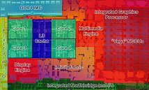
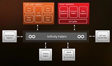
While "Summit Ridge" is the combination of two "Zen" CCX (quad-core CPU complex) units making up an 8-core CPU die that lacks integrated graphics, the "Raven Ridge" silicon combines one "Zen" CCX with an integrated graphics core based on the "Vega" architecture. AMD's new Infinity Fabric interconnect ferries data between the CCX and the iGPU, and not an internal PCIe link. The CCX houses four "Zen" CPU cores with 64 KB of L1I cache, 32 KB of L1D cache, 512 KB of dedicated L2 cache, and 4 MB of L3 cache shared between the four cores.The integrated graphics core is a different beast. It features similar (albeit scaled-down) front-end and back-ends from the "Vega 10" silicon, a similar video engine, and an SIMD area with 10 "Vega" next-gen compute units (NGCUs). This works out to a stream processor count of 640. Other key specifications include 40 TMUs, and 16 ROPs.
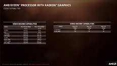
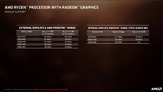
The video engine is now extremely capable, supporting hardware-accelerated decoding of CODECs such as VP9 10-bpc and HEVC 10-bpc at frame-rates of up to 240 for 1080p, and 60 for 4K UHD. It can also encode H.265 8-bpc at frame-rates of up to 120 at 1080p, and 30 at 4K UHD. You finally get to use the display connectors on your socket AM4 motherboards, as the iGPU supports DisplayPort 1.4 and HDMI 2.0b, with resolutions of up to 3840 x 2160 @ 60 Hz with HDR, 1440p @ 144 Hz, and 1080p @ 240 Hz.The Infinity Fabric interconnect forms the backbone of this silicon, as it connects all key components with each other, including the "Zen" CCX, the "Vega" iGPU, the display engine, the multimedia engine, the integrated northbridge, as well as the integrated southbridge (since like "Summit Ridge," "Raven Ridge" is an SoC).
The integrated northbridge features a dual-channel DDR4 integrated memory controller supporting up to 64 GB of memory at clock speeds of up to DDR4-3200; and a PCI-Express gen 3.0 root complex with a 28-lane budget. This means that besides the x4 A-Link chipset bus, the M.2 PCIe slots on typical machines will be wired to the APU. The integrated southbridge puts out two SATA 6 Gbps ports, and four USB 3.0 ports.
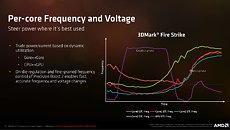
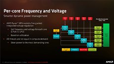
AMD seems so have increased the amount of power-gating on its silicon. Disabled or idling components triggered by lower power-states, are now power-gated (their power-supply cut off), and not clock-gated (their clock cadence cut-off). The chip is peppered with multiple LDO (low-dropout regulator) regions for the CCX, iGPU, and uncore regions, with a common VDD package rail for both the off-chip (on motherboard) and on-chip voltage controllers.Each component has a PG (power-gatable) region and an AON (always-on) region. The AON region is to make sure the component doesn't disappear from the address table while the system is running. The total max current requirements as a result of such as design change, have been reduced by as much as 36 percent.
The full AMD press deck with more technical info can be found at the end of this news post.


21 Comments on AMD "Raven Ridge" Silicon Detailed
ThinkPad A475 here I go! :D
Ot
I don't really need one but do want one , just to bench for a few days obviously.
Didn't A12-9800 and family do that already.
It seems a bit odd that Raven Ridge has more 'active' PCIE lanes in its root complex than Summit Ridge does.
You can pass on 4x from chipset like intel's DMI which is aaalmost PCI-E 3x but plug in an usb and you start killing NVME performance.
Amd have a dedicated NVME and another could be used through the chipset IE a 1500 mb/sec disk while having a 960 drive in the main M2 without issues.
none of the vendors deliver this but I feel AMD have the upper hand on this specific situation if by a small margin as other parts of the chipset is in some aspects lacking but overall it's designed well by AMD.
That's what I'm asking.
me too - esp re lanes. I hadread someplace that each zen core yields 4 lanes, so 28 lanes is good if true.
the next puzzle is how many lanes are used by the igp?
considering both cpu & gpu are fabric resident and capable, they have the option of using fewer lanes using the faster fabric protocol.
considering the usual 16 lanes for a gpu are freed up by the igp in the RR apu, RR should have stacks of lanes for nvme etc.