Tuesday, November 6th 2018

AMD Unveils "Zen 2" CPU Architecture and 7 nm Vega Radeon Instinct MI60 at New Horizon
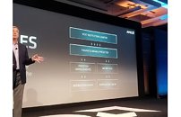
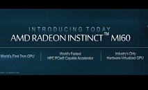
AMD today held its "New Horizon" event for investors, offering guidance and "color" on what the company's near-future could look like. At the event, the company formally launched its Radeon Instinct MI60 GPU-based compute accelerator; and disclosed a few interesting tidbits on its next-generation "Zen 2" mircroarchitecture. The Instinct MI60 is the world's first GPU built on the 7 nanometer silicon fabrication process, and among the first commercially available products built on 7 nm. "Rome" is on track to becoming the first 7 nm processor, and is based on the Zen 2 architecture.
The Radeon Instinct MI60 is based on a 7 nm rendition of the "Vega" architecture. It is not an optical shrink of "Vega 10," and could have more number-crunching machinery, and an HBM2 memory interface that's twice as wide that can hold double the memory. It also features on-die logic that gives it hardware virtualization, which could be a boon for cloud-computing providers.If you've been paying attention to our "Zen 2" coverage over the past couple of weeks, you would've read our recent article citing a Singapore-based VLSI engineer claiming that AMD could disintegrate the northbridge for its high core-count enterprise CPUs, in an attempt to make the memory I/O "truly" wide, without compromising on the idea of MCM CPU chiplets. All of that is true.
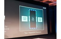
"Rome" is codename for a multi-chip module of four to eight 7 nm CPU dies, wired to a centralized die over InfinityFabric. This 14 nm die, called "I/O die," handles memory and PCIe, providing a monolithic 8-channel memory interface, overcoming the memory bandwidth bottlenecks of current-generation 4-die MCMs. The CPU dies and an I/O die probably share an interposer. Assuming each die has 8 CPU cores, "Rome" could have up to 64 cores, an 8-channel DDR4 memory interface, and a 96-lane PCI-Express gen 4.0 root-complex, per socket. If AMD has increased its core-count per CPU die, Rome's core count could be even higher.The broader memory I/O, assuming InfinityFabric does its job, could significantly improve performance of multi-threaded workloads that can scale across as many cores as you can throw at them, utilizing a truly broader memory interface. AMD also speaks of "increased IPC," which bodes well for the client-segment. AMD has managed to increase IPC (per-core performance), with several on-die enhancements to the core design.
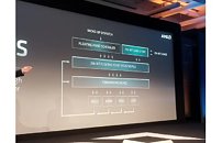
With "Zen" and "Zen+," AMD recognized several components on the core that could be broadened or made faster, which could bring about tangible IPC improvements. This includes a significantly redesigned front-end. Zen/Zen+ feature a front-end that's not much different than AMD's past micro-architectures. The new front-end includes an improved branch-predictor, a faster instruction prefetcher, an improved/enlarged L1 instruction cache, and an improved prefetcher cache (L2).
The number-crunching machinery, the floating point unit, also receives a massive overhaul. "Zen 2" features 256-bit FPUs, which are doubled in width compared to Zen. load/store/dispatch/retire bandwidths have been doubled over the current generation. These changes are massive. Given that even without these core-level changes, by simply improving cache latencies, AMD managed to eke out a ~3% IPC uplift with "Zen+," one can expect double-digit percentage IPC gains with "Zen 2." Higher IPC, combined with possible increased core counts, higher clock speeds, and power benefits of switching to 7 nm, complete AMD's "Zen 2" proposition.
Source:
Tom's Hardware
The Radeon Instinct MI60 is based on a 7 nm rendition of the "Vega" architecture. It is not an optical shrink of "Vega 10," and could have more number-crunching machinery, and an HBM2 memory interface that's twice as wide that can hold double the memory. It also features on-die logic that gives it hardware virtualization, which could be a boon for cloud-computing providers.If you've been paying attention to our "Zen 2" coverage over the past couple of weeks, you would've read our recent article citing a Singapore-based VLSI engineer claiming that AMD could disintegrate the northbridge for its high core-count enterprise CPUs, in an attempt to make the memory I/O "truly" wide, without compromising on the idea of MCM CPU chiplets. All of that is true.
"Rome" is codename for a multi-chip module of four to eight 7 nm CPU dies, wired to a centralized die over InfinityFabric. This 14 nm die, called "I/O die," handles memory and PCIe, providing a monolithic 8-channel memory interface, overcoming the memory bandwidth bottlenecks of current-generation 4-die MCMs. The CPU dies and an I/O die probably share an interposer. Assuming each die has 8 CPU cores, "Rome" could have up to 64 cores, an 8-channel DDR4 memory interface, and a 96-lane PCI-Express gen 4.0 root-complex, per socket. If AMD has increased its core-count per CPU die, Rome's core count could be even higher.The broader memory I/O, assuming InfinityFabric does its job, could significantly improve performance of multi-threaded workloads that can scale across as many cores as you can throw at them, utilizing a truly broader memory interface. AMD also speaks of "increased IPC," which bodes well for the client-segment. AMD has managed to increase IPC (per-core performance), with several on-die enhancements to the core design.
With "Zen" and "Zen+," AMD recognized several components on the core that could be broadened or made faster, which could bring about tangible IPC improvements. This includes a significantly redesigned front-end. Zen/Zen+ feature a front-end that's not much different than AMD's past micro-architectures. The new front-end includes an improved branch-predictor, a faster instruction prefetcher, an improved/enlarged L1 instruction cache, and an improved prefetcher cache (L2).
The number-crunching machinery, the floating point unit, also receives a massive overhaul. "Zen 2" features 256-bit FPUs, which are doubled in width compared to Zen. load/store/dispatch/retire bandwidths have been doubled over the current generation. These changes are massive. Given that even without these core-level changes, by simply improving cache latencies, AMD managed to eke out a ~3% IPC uplift with "Zen+," one can expect double-digit percentage IPC gains with "Zen 2." Higher IPC, combined with possible increased core counts, higher clock speeds, and power benefits of switching to 7 nm, complete AMD's "Zen 2" proposition.


57 Comments on AMD Unveils "Zen 2" CPU Architecture and 7 nm Vega Radeon Instinct MI60 at New Horizon
DDR4 supports up to 3200 MHz, Zen+ up to 2933 MHz and Intel up to 2666 MHz, all JEDEC 1.2V. But I haven't yet found any DIMMs supporting beyond 2666 MHz at 1.2V JEDEC spec.
DDR5 at 1.1V(?) is probably still far away.
AMD do have some impact with their Infinity fabric tied to the memory speed, but memory speed itself doesn't impact IPC.
Or the old pentiums getting vastly better performance by utilizing cache vs no cache previously ( this is the biggest example of feeding a cpu data = more ipc, cause it was so appearant at the time)
DDR4 memory is just L4 cache for a cpu, some tasks will see no improvements as long as the entire work can fit inside IE L1 cache
A bit simplified but should tell the story :)
As for 3200mhz kits on 1.2 v
www.gskill.com/en/product/f4-3200c16d-16gtzr
www.kingston.com/dataSheets/HX432C18FBK2_32.pdf
Although IPC does affect single core performance, it does not describe the final performance which is also affected by delays, timing, bandwidth and so on.
as far as I know threadripper SKU is based on epyc chips with some imperfection here and there
This makes me conclude that Rome runs at at least 10% lower clocks than Naples.
This has me so excited for Zen2. X2 the floating point performance, PCIE-4, hopefully a 10% IPC uplift, and maybe even a couple of hundred MHz clock speed uptick to close the deal! Great stuff, take my money AMD!
I suppose AMD want to keep the IPC improvements under their hat, as this 2X performance number was really like a Homer Simpson DOH! moment! Anything less than 2X performance, when core count is doubled, is a regression from Naples.
www.techpowerup.com/forums/threads/amds-zen-2-could-be-revealed-on-november-6th-next-horizon-event-scheduled.249151/#post-3934055
This is stuff people like to bash Intel about, but since you can't see into the future, you can never really guarantee a newly released CPU will work with boards built before it existed. So you must either change the socket (even if it's not really needed) or go through this revalidation, that may still leave you unable to use your old board if VRMs aren't up to the task or whatever.
Of course, you can reuse the socket if you stick to the exact same power spec. But more often than not, you're holding back the CPU by doing so.
Bottomline, reusing a socket is more complex than it seems. I'll happily take it when possible, but I won't fault chip makers when making me change the motherboard.
Also, the BIOS update route tends to work between incremental updates like Sandy to Ivy Bridge. It's trickier when you need to squeeze more cores into the same power envelope with voltage and current already set in stone.