Monday, March 9th 2020

Rumor: Intel to Introduce Big.Little Architecture for Desktop With Alder Lake-S, New LGA 1700 Socket
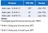
Hold on to your helmets: a wild rumor that Intel may be looking to introduce the same design considerations as they already did with their Lakefield architecture has appeared. According to momomo via Twitter (a user who has already shared many rumors and details in the PC hardware space) as well as some other sources, Intel is looking to bring a Big.Little-like design (which Intel calls Hybrid architecture) to the desktop platform in the form of Alder Lake-S, to be reportedly built on the 10 nm process. While Intel's Lakefield (especially geared for the mobile market) only sported four Atom (Intel's low power) Tremont cores combined with one high-performance Sunny Cove core, Alder Lake-S could sport as many as an 8+8 configuration, with a TDP currently set up to 80 W (and up to 125 W TDP is also set in the revealing slides with a disclosure regarding investigating performance scaling in up to 150 W TDP).
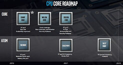
Should this actual Alder Lake-S product materialize in the 10 nm process, this could be a way for Intel to salvage what it can from the 10 nm process for the desktop platform. As we know from multiple reports on the state of Intel's 10 nm, yields and operating frequencies aren't close to what was expected, and Intel's CFO George Davis even said at last week's Morgan Stanley's Analyst Conference that their 10 nm process wouldn't be as profitable as even 22 nm, which does show that Intel is already looking past this process for their 7 nm deployment. A Big.Little design for a desktop architecture does seem like a more plausible design decision for a struggling process than a full 16-core monolithic die such as those Intel currently employs.The leaked slide also points to a new socket, LGA 1700, which would supersede the LGA 1200 that's being deployed with Comet Lake-S (10th gen) and which could feature support for Intel's Rocket Lake-S family (11th Gen). The leak also plays out a possible PCIe 4.0 support from Alder Lake-S, which could mean this is the first Intel architecture to sport this updated protocol, should it not debut with Rocket Lake-S already. Slightly logic, rational leaps mean that Intel could be looking at leveraging their Golden Cove (high performance) and Gracemont (Atom) CPU cores for this hybrid design.
Sources:
via Tom's Hardware, momomo @ Twitter, Ghost Motley @ Twitter, via Videocardz, Anandtech
Should this actual Alder Lake-S product materialize in the 10 nm process, this could be a way for Intel to salvage what it can from the 10 nm process for the desktop platform. As we know from multiple reports on the state of Intel's 10 nm, yields and operating frequencies aren't close to what was expected, and Intel's CFO George Davis even said at last week's Morgan Stanley's Analyst Conference that their 10 nm process wouldn't be as profitable as even 22 nm, which does show that Intel is already looking past this process for their 7 nm deployment. A Big.Little design for a desktop architecture does seem like a more plausible design decision for a struggling process than a full 16-core monolithic die such as those Intel currently employs.The leaked slide also points to a new socket, LGA 1700, which would supersede the LGA 1200 that's being deployed with Comet Lake-S (10th gen) and which could feature support for Intel's Rocket Lake-S family (11th Gen). The leak also plays out a possible PCIe 4.0 support from Alder Lake-S, which could mean this is the first Intel architecture to sport this updated protocol, should it not debut with Rocket Lake-S already. Slightly logic, rational leaps mean that Intel could be looking at leveraging their Golden Cove (high performance) and Gracemont (Atom) CPU cores for this hybrid design.


68 Comments on Rumor: Intel to Introduce Big.Little Architecture for Desktop With Alder Lake-S, New LGA 1700 Socket
Cpus can idle at 5 watts since sandy, big.little makes no sense in the way that it is implemented in smartphones, will it idle at 0.1 watt, or little core can just be used to offload some less demanding threads that would otherwise fragment and bottleneck the big core pipeline with lost clock cycles. I think Intel plans to move all the pcie lanes to the cpu substrate, including onchip thunderbolt usb to avoid the pcie4x bottleneck with PCH therefore the need for 500 more contacts.
This is exciting so long as they're priced appropriately but knowing Intel it's safe to say you'll probably get the exact opposite :slap:
Uhh, will this fit? How about this one? :D
if intel move the PCH part to the CPU, motherboard will become really cheap. so this is good.
Pathetic showing here. Intel shouldnt even bother until they have something to actually show performance wise.
With the little, big cores. Hmm. More pins. Hmm. two different cores two different power deliveries maybe more pins are needed for separate power delivery. Somehow this tells me it is not about performance increase it is about power savings due to 10nm insufficient manufacturing process. This kinda sounds to me, instead of increasing performance, giving more, faster cores, Intel goes smaller cores packed with regular calling (probably, since I haven't seen this as of yet) a better solution? For me it sound and looks like crippling product for obvious reasons. That also means Intel doesn't have a lot to offer against AMD.
Keep sticking to 2011 untill there are not enough pins anymore to push the data.
The idea for little cores on the desktop is somehow contradictory, though.
In gaming, for example, 8 normal cores can be used by the game, and 8 small cores by the OS.
But these small cores have much lower IPC and performance, and is it even meaningful to use such instead of normal cores that just switch between the tasks rapidly (in case the cores number is not enough) ?
As far as I'm concerned, they can shove this lake right up there with the rest of the watery graveyard. I'm approaching Intel like I do AMD GPU: Product pls!
When I see it I believe it. I don't take in on faith.
Anyway it is weird what Intel is offering and what rumors say. Hard to see any advantages with these big little cores.
Edit:
4-core 14nm Apollo Lake die is roughly 9 x 10.2 mm - 91.4 mm^@. From that die, 4 Goldmont cores are 11mm^2.
For comparison:
- One 7nm Zen2 core (without L3) is 3.64mm^2 - 7nm scaling over 14nm is about 60%.
- One 14/12nm Zen/Zen+ core is about 7mm^2.
- One 14nm Skylake core is about 8.73 mm^2 - Kaby Lake, Coffee Lake/Refresh and supposedly Comet Lake are all about the same.
AMD already has a big 16-core CPU, why bother with this one?
Also, the implementation will take a lot of time to develop, leading to more issues with the OS.
Interesting concept, but I think it will flop really soon.
I can totally see the Little core serve a purpose for idle usage with the big ones being shut off completely. You only need a few hundred mhz to run some sensors, gyro, gps, etc, perhaps even a simple browser or background process, push services from the OS. This will give Intel an edge in battery life, probably greater than anything AMD can bring to Zen chiplets atm.
10nm ain't happening, that is for sure, and 14nm won't cut it here for battery life. Those laptop CPUs are fast becoming Atoms with a ridiculous turbo the way they're going with baseclocks... heck even the desktop CPUs are starting to lean that way. Not touching these with a 10nm pole tho.