Wednesday, September 23rd 2020

Intel 14 nm Node Compared to TSMC's 7 nm Node Using Scanning Electron Microscope
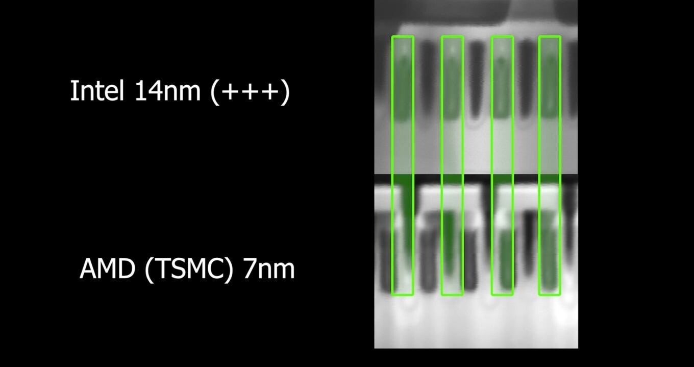
Currently, Intel's best silicon manufacturing process available to desktop users is their 14 nm node, specifically the 14 nm+++ variant, which features several enhancements so it can achieve a higher frequencies and allow for faster gate switching. Compare that to AMD's best, a Ryzen 3000 series processor based on Zen 2 architecture, which is built on TSMC's 7 nm node, and you would think AMD is in clear advantage there. Well, it only sort of is. German hardware overclocker and hacker, der8auer, has decided to see how one production level silicon compares to another, and he put it to the test. He decided to use Intel's Core i9-10900K processor and compare it to AMD's Ryzen 9 3950X under a scanning electron microscope (SEM).
First, der8auer took both chips and detached them from their packages; then he proceeded to grind them as much as possible so SEM could do its job of imaging the chips sans the substrate and protective barrier. This was followed by securing the chips to a sample holder using an electrically conductive adhesive to improve penetration of the high energy electrons from the SEM electron gun. To get as fair a comparison as possible, he used the L2 cache component of both processors as they are usually the best representatives of a node. This happens because the logic portion of the chip differs according to architecture; hence, level two cache is used to get a fair comparison - it's design is much more standardized.
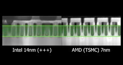

The results? Well, the Intel 14 nm chip features transistors with a gate width of 24 nm, while the AMD/TSMC 7 nm one has a gate width of 22 nm (gate height is also rather similar). While these are not much different, TSMC's node is still much denser compared to Intel's - TSMC's 7 nm produces chips with a transistor density around 90 MT/mm² (million transistors per square millimeter), which is comparable in density to Intel's 10 nm node used on recent mobile processors. Below you can see the SEM images and comparison made. For more information and details please head over to the source.
Another interesting thing to note here, the gate width is not following the naming scheme as you might have expected. The 14 nm transistor isn't 14 nm in width, and the 7 nm transistor isn't 7 nm wide. The naming of the node and actual size of the node have had a departure a long time ago, and the naming convention is really up to the manufacturer - it's become more of a marketing gimmick than anything else. This is the reason researchers have already proposed another density metric for semiconductor technology other than pure "nm" terms.
Source:
Der8auer (YouTube)
First, der8auer took both chips and detached them from their packages; then he proceeded to grind them as much as possible so SEM could do its job of imaging the chips sans the substrate and protective barrier. This was followed by securing the chips to a sample holder using an electrically conductive adhesive to improve penetration of the high energy electrons from the SEM electron gun. To get as fair a comparison as possible, he used the L2 cache component of both processors as they are usually the best representatives of a node. This happens because the logic portion of the chip differs according to architecture; hence, level two cache is used to get a fair comparison - it's design is much more standardized.

Another interesting thing to note here, the gate width is not following the naming scheme as you might have expected. The 14 nm transistor isn't 14 nm in width, and the 7 nm transistor isn't 7 nm wide. The naming of the node and actual size of the node have had a departure a long time ago, and the naming convention is really up to the manufacturer - it's become more of a marketing gimmick than anything else. This is the reason researchers have already proposed another density metric for semiconductor technology other than pure "nm" terms.
49 Comments on Intel 14 nm Node Compared to TSMC's 7 nm Node Using Scanning Electron Microscope
even worse than we thought :laugh:
Notice the transistor density of 7nm is much higher than that of Intel's. So while the gate size may be close to the same the density also matters.
On a side note, the density may be part of the reason AMD is struggling with breaking the 5Ghz barrier with this node, the power density increases as transistor density increases, meaning fewer watts per transistor allowed due to thermal constraints. The only way out is to shrink the transistors and leave more space around them to dissipate the heat.
Why do people think samsung had a 7nm process since 2018 because they advertise it to the public even when it's was basically not usable
Different logic/i.o/cache/memory all comes in different densities and all can end up on the same chip.
Also just because they make a 2 chips on the same 7nm process doesn't mean the 2 chips with similar logic made by different companies are the same. They can end up being different sizes because there are more things to consider when designing a chip.
I think of it as there will be more tunneling and less conduction. Like hamr tech in hard drives, conduction will take facilitation to proceed in higher gate resistances than previously available.
That's not a non-trivial advantage, but definitely less than I expected from 14nm > 7nm based on the marketing lies.
Next I want to know how much of a jump TSMC 28 > 14nm was. We were stuck on 28nm for so long that I thought Moore's Law was completely dead back then.Source? What has he done to earn his troll status - I don't really follow him closely....
If you look into Intel 10nm, Tiger Lake is their 2nd generation "10nm" node and it has most of the same characteristics as TSMCs 2nd generation "7nm" node. It is more dense than TSMC 1st gen 7nm which is used on Zen 2.
This means that technically Tiger Lake @ 10nm+ will be on a superior node to Zen 2 7nm (first gen node).
IIRC Zen 3 is to use TSMC 7nm 2nd gen, which is on par with Intel 10nm+ (or 10nm superfin or w/e they are calling it now).
The problem of course is that Intel has no plans to use 10nm+ for desktop. This is where their real crunch will come in, while they use 10nm+ to defend their laptop and server space, they've deprecated the desktop space in importance until 2022 when Intel 7nm (5nm TSMC equivalent) comes online.
I guess we will know in 3-6 months when we can see Rocket Lake (Intel 14nm) vs Zen 3 (TSMC 2nd gen 7nm).
That is what I've been telling. The saving on interconnect dynamic power is almost the same. That makes them equal on power efficiency, but that does not cover the rest of transistor benchmarks.
They cannot push more current, but can maintain the same resistance.
In light of the notion of this thread, I honestly think Samsung can disrupt the market. Gate features are the most developed backbones of the industry. The question is who will seperate the wheat from the chaff - tunneling effects are best exploited when there is not a single bandgap like the blinders are semiclosed(I totally make it up, astroturf style).
And Intel 10nm is MORE dense than Samgung and TSMC 1st/2nd gen 7nm :
Here's the 12-16nm node. Intel's 14nm is more dense than any of the competitors "12nm-16nm" nodes. It's *a lot* closer to Samsung's "10nm" node than Samungs 10nm is to Intel's 10nm node.
Point here being these node names are utter marketing garbage. Meaningless marketing BS.
I just tried to entertain a fresh perspective. 14nm good 10/7nm bad > reassess motives, retool the gate physics kinda stuff. I do think MBC fet is not classical physics stuff, but this is coming from a non-EE guy.
Like when you rub glass rod(insulator) with a cloth, these new kinds of gates will find ways to push charge and not current over higher insulation gates, like sieves letting water through and not vibrating rocks. You may say I'm a dreamer, but eventhough the market is dead for hdds, hamr is still a thing. They indeed launched the crap smr before that, true, but this is much the same as hamr which is coming down the line nonetheless.
Electric current and magnetic resistance is somewhat coupled, so they say. It ought to prevent current if they can hone in on the magnetic component.
They should have used names like 13nm and 15nm for the so called fake "10nm, 11nm and 8nm".
Since the nanometer measure is more marketing, can someone tell me what the real nm size is for TSMC 5nm nodes are?
Other questions
From what I have read, it seems that the insane performance of the M1 Macbook might have more to do with the jump from Intel 10nm to TSMC 5nm. This would potentially provide somewhere around a 35% speed improvement, 65% less power, and a 3.3X density improvement even without using a new architecture. This would mean that M1 performance might have little to do with ARM vs x86. I mean, the architectures are not very different in modern days.
ARMv8.1-M from Feb 2019 added 150 new instructions for signal processing and vector math. Group some of these instructions together into common operations and they start to look like CISC. AMD and Intel now use Microcode which takes a complex instruction and breaks it up into its component tasks which starts to look like the instruction pipeline on a RISC chip. RISC chips can actually require a large cache.
So how is Apple's design different than native ARM I wonder? There are limits to what its ARM license allows. Even Apple can’t radically alter the ARM instruction set or the programmer’s model without permission from ARM.
Does anyone really think that the original 10nm was anything but a complete disaster? Perhaps the article would help change minds of some of these skeptics.
www.anandtech.com/print/16107/what-products-use-intel-10nm-superfin-demystified