Friday, September 25th 2020
RTX 3080 Crash to Desktop Problems Likely Connected to AIB-Designed Capacitor Choice
Igor's Lab has posted an interesting investigative article where he advances a possible reason for the recent crash to desktop problems for RTX 3080 owners. For one, Igor mentions how the launch timings were much tighter than usual, with NVIDIA AIB partners having much less time than would be adequate to prepare and thoroughly test their designs. One of the reasons this apparently happened was that NVIDIA released the compatible driver stack much later than usual for AIB partners; this meant that their actual testing and QA for produced RTX 3080 graphics cards was mostly limited to power on and voltage stability testing, other than actual gaming/graphics workload testing, which might have allowed for some less-than-stellar chip samples to be employed on some of the companies' OC products (which, with higher operating frequencies and consequent broadband frequency mixtures, hit the apparent 2 GHz frequency wall that produces the crash to desktop).
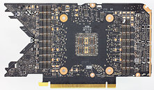
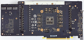
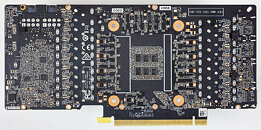
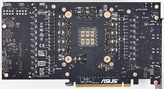
Another reason for this, according to Igor, is the actual "reference board" PG132 design, which is used as a reference, "Base Design" for partners to architecture their custom cards around. The thing here is that apparently NVIDIA's BOM left open choices in terms of power cleanup and regulation in the mounted capacitors. The Base Design features six mandatory capacitors for filtering high frequencies on the voltage rails (NVVDD and MSVDD). There are a number of choices for capacitors to be installed here, with varying levels of capability. POSCAPs (Conductive Polymer Tantalum Solid Capacitors) are generally worse than SP-CAPs (Conductive Polymer-Aluminium-Electrolytic-Capacitors) which are superseded in quality by MLCCs (Multilayer Ceramic Chip Capacitor, which have to be deployed in groups). Below is the circuitry arrangement employed below the BGA array where NVIDIA's GA-102 chip is seated, which corresponds to the central area on the back of the PCB.In the images below, you can see how NVIDIA and it's AIBs designed this regulator circuitry (NVIDIA Founders' Edition, MSI Gaming X, ZOTAC Trinity, and ASUS TUF Gaming OC in order, from our reviews' high resolution teardowns). NVIDIA in their Founders' Edition designs uses a hybrid capacitor deployment, with four SP-CAPs and two MLCC groups of 10 individual capacitors each in the center. MSI uses a single MLCC group in the central arrangement, with five SP-CAPs guaranteeing the rest of the cleanup duties. ZOTAC went the cheapest way (which may be one of the reasons their cards are also among the cheapest), with a six POSCAP design (which are worse than MLCCs, remember). ASUS, however, designed their TUF with six MLCC arrangements - there were no savings done in this power circuitry area.It's likely that the crash to desktop problems are related to both these issues - and this would also justify why some cards cease crashing when underclocked by 50-100 MHz, since at lower frequencies (and this will generally lead boost frequencies to stay below the 2 GHz mark) there is lesser broadband frequency mixture happening, which means POSCAP solutions can do their job - even if just barely.
Source:
Igor's Lab
Another reason for this, according to Igor, is the actual "reference board" PG132 design, which is used as a reference, "Base Design" for partners to architecture their custom cards around. The thing here is that apparently NVIDIA's BOM left open choices in terms of power cleanup and regulation in the mounted capacitors. The Base Design features six mandatory capacitors for filtering high frequencies on the voltage rails (NVVDD and MSVDD). There are a number of choices for capacitors to be installed here, with varying levels of capability. POSCAPs (Conductive Polymer Tantalum Solid Capacitors) are generally worse than SP-CAPs (Conductive Polymer-Aluminium-Electrolytic-Capacitors) which are superseded in quality by MLCCs (Multilayer Ceramic Chip Capacitor, which have to be deployed in groups). Below is the circuitry arrangement employed below the BGA array where NVIDIA's GA-102 chip is seated, which corresponds to the central area on the back of the PCB.In the images below, you can see how NVIDIA and it's AIBs designed this regulator circuitry (NVIDIA Founders' Edition, MSI Gaming X, ZOTAC Trinity, and ASUS TUF Gaming OC in order, from our reviews' high resolution teardowns). NVIDIA in their Founders' Edition designs uses a hybrid capacitor deployment, with four SP-CAPs and two MLCC groups of 10 individual capacitors each in the center. MSI uses a single MLCC group in the central arrangement, with five SP-CAPs guaranteeing the rest of the cleanup duties. ZOTAC went the cheapest way (which may be one of the reasons their cards are also among the cheapest), with a six POSCAP design (which are worse than MLCCs, remember). ASUS, however, designed their TUF with six MLCC arrangements - there were no savings done in this power circuitry area.It's likely that the crash to desktop problems are related to both these issues - and this would also justify why some cards cease crashing when underclocked by 50-100 MHz, since at lower frequencies (and this will generally lead boost frequencies to stay below the 2 GHz mark) there is lesser broadband frequency mixture happening, which means POSCAP solutions can do their job - even if just barely.

297 Comments on RTX 3080 Crash to Desktop Problems Likely Connected to AIB-Designed Capacitor Choice
Real life example. Let's imagine you are GPU and jumping up is equivalent to computing a frame in the game. You are healthy and strong GPU. You jump lightweight, you can jump 100 times an hour (e.g. 100 fps :D) no sweat. This is when you have no capacitive and inductive loading case. Now we add 1kg of weights to your backpack. You can jump only 80 times an hour, because now its harder to jump with that extra weight added (this is when we have just tiny MLCCs around). Let's add 10kg of weights.. this is some polymer "POSCAP"s around... Now you jump only 50 times, it's getting heavy to bring all that mass up, and then slow it down when you land... Now add VRM inductors and bulk capacitors...another 40 kg weight.... oops...you can barely jump at 5 times.... soooo heavy..... so sloooow.... This is PDN for dummies :D Power designer job is to optimize weights on each step, so system as a whole handle workloads well. And you don't need to know about muscle cell composition, neurons operation or immune system hormones or even blood flow (inner workings of GPU) when you doing jumps...
And while GPU operate at 2.1GHz (which is interesting question on itself, because internally clocks are not 2.1 GHz everywhere ;), current pulses and draw spikes that fast will never reach PCB level. This is ABC of circuit design and PDN design. The higher frequency is, the smaller (physical) sizes are. You cannot have current suddenly switch on huge copper sheet polygon with a GHz rate due to huge inductance and capacitance between PCB layers. That is why you have those teeeeny 01005 capacitors around the GPU/CPU dies and why you have layers inside BGA package (which is structured exactly like PCB, but smaller). Those are first line of "defense" against switching currents, and they filter GHz current transients. What reaches PCB right behind the core is tens and hundreds MHz rate tops. And having 1GHz or just 2.5GHz oscilloscope (to be sure) with PROPER probing is enough to measure 100MHz power spikes and ripple. Such scope is available at every AIB lab, nothing special.
Here's some basic documents on the topic: www.intel.com/content/www/us/en/programmable/support/support-resources/support-centers/signal-power-integrity/power-distribution-network.html
It is ALTERA (now Intel) page on PDN. It's about FPGA power design but same principle applies to CPU or GPU too. Please note that plot does not extend post 1 GHz ;). There is nice PDF going over basics too.
See those notches? Each notch is a particular "capacitor" (in reality its a combined inductance+capacitance+impedance). First notch would be bulk caps, then big MLCC, then smaller MLCC, than tiny MLCCs sprinkled everywhere on the PCB, then GPU package with onboard caps, and finally at tens/hundreds of MHz capacitance/inductance of package and die power networks itself.
Another plot showing notches from different decoupling "sources". Plot here shows impedance from DC to 10GHz. You can see on-package capacitors kick off at 100MHz+ mark, while on-die structures handle 1GHz+ range. Again, no 10GHz+ stuff or ASIC design knowledge required here, because while in theory we can probe inside GPU (and I'm sure NVIDIA R&D engineers do that during design of the chip with their multi-M$ equipment and fancy tools), it's irrelevant for PCB designer or AIB point of view for VRM/power design, because they are given chips as a whole, and have zero control over chip operation. But have requirements and target impedance and voltage margins, which must be met by PCB designer and VRM tuning/components selection.
These are just random pics on topic from 1 minute googling.
Also there is whole lot of another factors, which are way more important than decoupling banks. Such as load-line tuning, VRM stability and RFI/EMI aware design. If any if these are bad, than you can have perfect decoupling scheme and layout in the world, but your product will be unstable mess as a whole. It's like spending 10000$ on audiofoolery mains power cable (fancy MLCC arrays), while you have aluminum AWG22 wiring inside the wall (bad power settings, poor stability for VRM PWM controller) on the other side of the outlet :D Great job for capacitors , A+ for efforts, but still F for overclocking and meeting specs...
Btw, all of this is perfect example on HOW and WHY overclocking, especially liquid nitrogen overclocking is nice and helpful tool. If you just test design on NVIDIA spec conditions, you may never reach the poor stability VRM region. While pushing chip to 30-50% higher than the spec will instantly reveal instabilities and deficiency of the power design. And believe, here I am not talking about "which AIB card got more phases" or "whose MOSFET have 90A rating instead of 60A", but actual things that matter, like VRM stability, correct phase-shifts, balancing load, and of-course decoupling networks ;).
When I was working on all KPE cards, PDN experiments and measurements are what took most time, tuning for all those things in system level. And I didn't need to use fancy 10GHz oscilloscope for these tests. Okay, I'm done :DBingo! My point precisely, I am not convinced at all that culprit is in using few MLCC or polymer cap behind a GPU, it's just misinformation and guesswork spread by one blogger IMHO.I do have expensive tools, and one can buy 1GHz oscilloscope and decent differential probes from eBay for $3-6k without problem to measure and tune power delivery. But obviously I am not going into practice of it all, as I don't work in consumer field anymore. It is interesting problem to look at however, no denial about that, just not interesting enough :D.
And most likely we will never know the root cause, because stuff like this is never shown publicly, because this is bread and butter of AIBs that differentiate ones who just copy designs from ones who actually design things better by having how-to. So those well-paid engineers will need to keep their NDAs and not say a word. :)
industrial.panasonic.com/ww/products/capacitors/polymer-capacitors/poscap
Like "Core i7" for some Intel processors.
Enhance...
Enhance...
the evga statement posted by jacob seems to be supportting the "guesswork" from that blogger, what do you think?
forums.evga.com/Message-about-EVGA-GeForce-RTX-3080-POSCAPs-m3095238.aspx
i have seen some ppl saying after shutmod or flashing xoc bios on watercooled 2080ti/titan, they can get 21XX~22XX mhz for binned gpu in games/benchmarks.
what is your guess on rtx3090 kingpin? should we expect such level of oc on 3080/3090?
thanks.
Anyway whoever is going to be buying a 3080 (new or used) on ebay will have to be extremely careful and possibly ask for a visual inspection of the pcb to make sure he/she isn't paying the full whack for an early batch unit.
So you say,certain production cost is all about how components are placed,but ignoring the cost(=quality) of the given components?
Actually you are so clueless..but then you shouldnt act otherwise.
Later edit: after posting this reply now it took me to a section of the site where there is an "unwatch" button. The original page where I was reading the comments didn't have either "watch" or "unwatch":
www.techpowerup.com/272591/rtx-3080-crash-to-desktop-problems-likely-connected-to-aib-designed-capacitor-choice
Hah ninja edit ;)
and yes I bought a Radeon 7 lol
BTW lets hope a load of people using bots to buy up all the cards get stuck with the early batch's. That would be perfect.
www.proshop.dk/Grafikkort/ASUS-GeForce-RTX-3080-TUF-10GB-GDDR6X-RAM-Grafikkort/2876763
www.proshop.dk/Grafikkort/ASUS-GeForce-RTX-3080-TUF-OC-10GB-GDDR6X-RAM-Grafikkort/2876861
www.proshop.dk/Grafikkort/ASUS-GeForce-RTX-3080-ROG-STRIX-10GB-GDDR6X-RAM-Grafikkort/2876857
@OneMoar & @Rado D
I'm redirecting that video right back at you the two of you and I'm going to suggest that you go do some "moar" reading, paying careful attention to context. There are a few subtleties you both seem to be missing.