Friday, September 25th 2020
RTX 3080 Crash to Desktop Problems Likely Connected to AIB-Designed Capacitor Choice
Igor's Lab has posted an interesting investigative article where he advances a possible reason for the recent crash to desktop problems for RTX 3080 owners. For one, Igor mentions how the launch timings were much tighter than usual, with NVIDIA AIB partners having much less time than would be adequate to prepare and thoroughly test their designs. One of the reasons this apparently happened was that NVIDIA released the compatible driver stack much later than usual for AIB partners; this meant that their actual testing and QA for produced RTX 3080 graphics cards was mostly limited to power on and voltage stability testing, other than actual gaming/graphics workload testing, which might have allowed for some less-than-stellar chip samples to be employed on some of the companies' OC products (which, with higher operating frequencies and consequent broadband frequency mixtures, hit the apparent 2 GHz frequency wall that produces the crash to desktop).
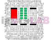
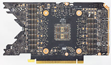
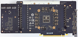
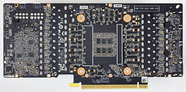
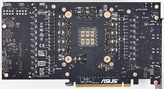
Another reason for this, according to Igor, is the actual "reference board" PG132 design, which is used as a reference, "Base Design" for partners to architecture their custom cards around. The thing here is that apparently NVIDIA's BOM left open choices in terms of power cleanup and regulation in the mounted capacitors. The Base Design features six mandatory capacitors for filtering high frequencies on the voltage rails (NVVDD and MSVDD). There are a number of choices for capacitors to be installed here, with varying levels of capability. POSCAPs (Conductive Polymer Tantalum Solid Capacitors) are generally worse than SP-CAPs (Conductive Polymer-Aluminium-Electrolytic-Capacitors) which are superseded in quality by MLCCs (Multilayer Ceramic Chip Capacitor, which have to be deployed in groups). Below is the circuitry arrangement employed below the BGA array where NVIDIA's GA-102 chip is seated, which corresponds to the central area on the back of the PCB.In the images below, you can see how NVIDIA and it's AIBs designed this regulator circuitry (NVIDIA Founders' Edition, MSI Gaming X, ZOTAC Trinity, and ASUS TUF Gaming OC in order, from our reviews' high resolution teardowns). NVIDIA in their Founders' Edition designs uses a hybrid capacitor deployment, with four SP-CAPs and two MLCC groups of 10 individual capacitors each in the center. MSI uses a single MLCC group in the central arrangement, with five SP-CAPs guaranteeing the rest of the cleanup duties. ZOTAC went the cheapest way (which may be one of the reasons their cards are also among the cheapest), with a six POSCAP design (which are worse than MLCCs, remember). ASUS, however, designed their TUF with six MLCC arrangements - there were no savings done in this power circuitry area.It's likely that the crash to desktop problems are related to both these issues - and this would also justify why some cards cease crashing when underclocked by 50-100 MHz, since at lower frequencies (and this will generally lead boost frequencies to stay below the 2 GHz mark) there is lesser broadband frequency mixture happening, which means POSCAP solutions can do their job - even if just barely.
Source:
Igor's Lab
Another reason for this, according to Igor, is the actual "reference board" PG132 design, which is used as a reference, "Base Design" for partners to architecture their custom cards around. The thing here is that apparently NVIDIA's BOM left open choices in terms of power cleanup and regulation in the mounted capacitors. The Base Design features six mandatory capacitors for filtering high frequencies on the voltage rails (NVVDD and MSVDD). There are a number of choices for capacitors to be installed here, with varying levels of capability. POSCAPs (Conductive Polymer Tantalum Solid Capacitors) are generally worse than SP-CAPs (Conductive Polymer-Aluminium-Electrolytic-Capacitors) which are superseded in quality by MLCCs (Multilayer Ceramic Chip Capacitor, which have to be deployed in groups). Below is the circuitry arrangement employed below the BGA array where NVIDIA's GA-102 chip is seated, which corresponds to the central area on the back of the PCB.In the images below, you can see how NVIDIA and it's AIBs designed this regulator circuitry (NVIDIA Founders' Edition, MSI Gaming X, ZOTAC Trinity, and ASUS TUF Gaming OC in order, from our reviews' high resolution teardowns). NVIDIA in their Founders' Edition designs uses a hybrid capacitor deployment, with four SP-CAPs and two MLCC groups of 10 individual capacitors each in the center. MSI uses a single MLCC group in the central arrangement, with five SP-CAPs guaranteeing the rest of the cleanup duties. ZOTAC went the cheapest way (which may be one of the reasons their cards are also among the cheapest), with a six POSCAP design (which are worse than MLCCs, remember). ASUS, however, designed their TUF with six MLCC arrangements - there were no savings done in this power circuitry area.It's likely that the crash to desktop problems are related to both these issues - and this would also justify why some cards cease crashing when underclocked by 50-100 MHz, since at lower frequencies (and this will generally lead boost frequencies to stay below the 2 GHz mark) there is lesser broadband frequency mixture happening, which means POSCAP solutions can do their job - even if just barely.

297 Comments on RTX 3080 Crash to Desktop Problems Likely Connected to AIB-Designed Capacitor Choice
What is the only logical conclusion here? I leave it to you...
I hope that tomorrow Nvidia relases an statement of this issue and add some information about it, because today all is rumour and noise... if FE are having same problems, I want to doubt that this is a HW problem...
Did they push the silicon too far from the start? Then, they will have to release updated firmwares with some downclock or something like that...
Sticking with my 1080 for now, I'll wait till the 20 series sells dirt cheap on eBay before pulling the trigger!
basically every corner they cut they can and its just enough to push the stability envelope past the limit when you are trying to hit that magical 2Ghz marketing number
ever since Nvidia started making there own boards the AIBS have been cutting every corner possible if you want a reliable card, you buy the Nvidia made one(unless you wanna spend the money for the absolute top tier cards like a Strix, Hall of Fame, k1ngpin)
this is a complete reversal from how it used to be
it used to be AIB cards offered more bang for the buck with better overclocking and better cooling this is frankly no longer the case and the short of it is unless Nvidia relaxes some of the restrictions AIBS only continued reason to exist is to make cards for Nvidia
We are not shooting here NVIDIA's legs, we simply trying to get a bit of encyclopedia understanding of what when wrong.
microsecondmilliseconds latency, afaik.This could be related to slow responses to monitored events, wouldn't you say? We are talking about 2.5ghz chips that were previously impossible when these monitoring software first took over.
www.extremetech.com/gaming/170542-amds-radeon-r9-290-has-a-problem-but-nvidias-smear-attack-is-heavy-handed/2
PS: I indeed think it is as simple as that, vdroop that is occurring quicker than 30 times a second which is above the monitoring resolution. As with cpu overclocking, a higher base voltage, or LLC would further complicate the power requirements. The solution is definitely good, but it has to be inside the frameset of parametrization. Something is voiding the algorithm.
a) AIB to refer to 'non reference' graphics card designs.
b) An AIB supplier or an AIB partner is a company that buys the AMD (or Nvidia) Graphics Processor Unit to put on a board and then bring a complete and usable Graphics Card or AIB to market.
20 years ago we did complain (me too) that NVIDIA was flooding the market with VGA card releases when the performance at positive scaling was just 12%.
Series TNT and then TNT2 and and and .... more money spend with out real benefit.
Since 2012 I did stop to be a close follower of 3D cards development, I did use the storage ability of my brain at other by far more productive thoughts.
Development of software this is always a second support step, if NVIDIA did not add relative power usage monitor sensors, no one would be able to see power related information's (electrical measurements).
If only we still had @The Stilt around.
The method I would suggest at a big die gpu is still the same - try incrementally at 50MHz steps and see if there is a cutoff point where this behaviour starts. 1600 MHz, 1650 MHz, 1700 MHz... I'm not a metrologist which I highly respect as a science, but I can at least go down to the minimum resolution(1 MHz) until problem begins.
I used to combine ATi Tray Tools since not most software came with its error counter. I would monitor the gpu frequency time log in its overclock test and watch for the card to spit out errors in ATT(you had to select osd error check to monitor it live on the lower corner).
It was great fun, but such old software has a habit of damaging your card when continuously running at 5000fps, lol.
I cannot be of much other help outside of pointing out which software I used to get a frame of reference.
I hope they fix it because it rekindles the good old times I spent dialing just single digits in MSI Afterburner.
My current AMD HD5770 this has an internal scanning method so to determine max OC limits all by it self.
I never care to learn the scaling up in Megahertz steps.
RTX 3000 and what ever will follow after it, this is a different animal, I am sensing that Major OC software and utilities these will not be required any more.
This new hardware it is now made to restrict careless handling from the side of users.
Its a new car with no gears stick, and with a limiter at allowed top speed.
Anyone whom disagree with the new reality he should never get one.
Since this is about power delivery, it has to "match" the power requirement of the normal operating bevaviour.
Since the testing utility is good, but doesn't test at the same temperature ranges an overclocked case can rise up to, we'll have to reserve ourselves to more moderate speeds than what the utility can have us believe.
This is why I mentioned ATT, it follows the same fan temperature curve in the normal operating behaviour.
This is mainly about vdroop and temperature beyond that. The way I used it was, I would start the 3d renderer, let go of tuning a little bit, and wait until the card reached previously noted temperature points where it destabilized and switch to 'manual' from there(never expected ATT to sound this cool).
The leakiness brought about by temperature, inclining power requirements due to faster shader operation would get you a sweet spot where this cutoff was too easy to pinpoint. From there, I would play either with the fan curve, or voltage, or if on the cpu with LLC(you couldn't pick its temperature gradient if you didn't log everything up until here), but basically I find it more exciting to bust cards using this method than to use them daily, lol.
As the saying goes .... good things come to those who wait .... if the PCBs are indeed faulty, they will be redesigned and those who choose to wait won't have to deal with a 1st stepping design issue. The alleged "cutting corners" by AIBs is simply not supported bu history... the AIB offerings, for the most part, have always outperformed the reference and FE designs. Yes, we have the deficient EVGA designs (9xx heat sink, 1xxx missing thermal pads, 2xxx Black series non "A" GPU) which didn't measure up but that's the exception rather than the rule. I have commented a few times that "what did MSI do differently that they are the only card to deliver more fps than the FE. I did note that they had one of the lowest power limits ... perhaps the problem arises when that limit is exceeded ? In any case, hopefully folks who were unable to snag one before they were sold out, will now cancel the orders, sit and wait till the problem is defined, which cards it affects and the issued addressed in later offferings