Wednesday, September 21st 2022

NVIDIA RTX 4090 Doesn't Max-Out AD102, Ample Room Left for Future RTX 4090 Ti
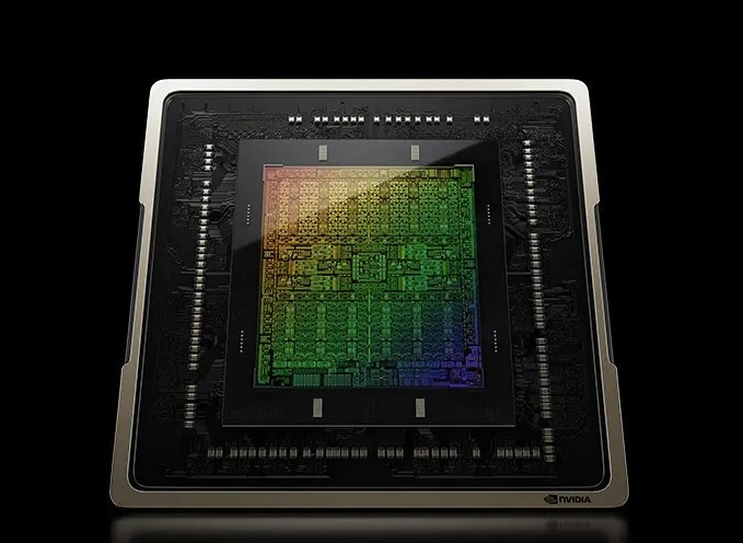
The AD102 silicon on which NVIDIA's new flagship graphics card, the GeForce RTX 4090, is based, is a marvel of semiconductor engineering. Built on the 4 nm EUV (TSMC 4N) silicon fabrication process, the chip has a gargantuan transistor-count of 76.3 billion, a nearly 170% increase over the previous GA102, and a die-size of 608 mm², which is in fact smaller than the 628 mm² die-area of the GA102. This is thanks to TSMC 4N offering nearly thrice the transistor-density of the Samsung 8LPP node on which the GA102 is based.
The AD102 physically features 18,432 CUDA cores, 568 fourth-generation Tensor cores, and 142 third-generation RT cores. The streaming multiprocessors (SM) come with special components that enable the Shader Execution Reordering optimization, which has a significant performance impact on both raster- and ray traced graphics rendering performance. The silicon supports up to 24 GB of GDDR6X or up to 48 GB of GDDR6+ECC memory (the latter will be seen in the RTX Ada professional-visualization card), across a 384-bit wide memory bus. There are 568 TMUs, and a mammoth 192 ROPs on the silicon. The RTX 4090 is carved out of this silicon by enabling 16,384 out of 18,432 CUDA cores. 512 out of 568 Tensor cores, 512 out of 568 TMUs, 128 out of 142 RT cores, and unless NVIDIA has touched the ROP count, it could remain at 192. The memory bus is maxed out, with 24 GB of 21 Gbps GDDR6X memory across the 384-bit bus-width. In creating the RTX 4090, NVIDIA has given itself a 10% headroom in the number-crunching machinery, from which to carve out future SKUs such as the possible RTX 4090 Ti. Until that SKU is needed in the product-stack, NVIDIA will use this 10% margin toward harvesting the AD102 silicon.
The AD102 physically features 18,432 CUDA cores, 568 fourth-generation Tensor cores, and 142 third-generation RT cores. The streaming multiprocessors (SM) come with special components that enable the Shader Execution Reordering optimization, which has a significant performance impact on both raster- and ray traced graphics rendering performance. The silicon supports up to 24 GB of GDDR6X or up to 48 GB of GDDR6+ECC memory (the latter will be seen in the RTX Ada professional-visualization card), across a 384-bit wide memory bus. There are 568 TMUs, and a mammoth 192 ROPs on the silicon.
27 Comments on NVIDIA RTX 4090 Doesn't Max-Out AD102, Ample Room Left for Future RTX 4090 Ti
So, this is how Nvidia's lack of TSMC works, you mean. Because now we're back on TSMC and suddenly we cán get decent VRAM capacities (all on GDDR6X this time, btw, and all but the largest capacities under 300W) from the get-go alongside numerous core/transistor count improvements and an overall performance boost.
Stop fooling yourself. This was clear since launch and was then proven by Nvidia's own release cadence plus what came before and after Ampere, now. The consensus was, is and will be that early Ampere is the all time low in relative core power to VRAM of the last decade; numbers don't lie. Its also the only gen built on Samsung, mind, only the consumer line, the real stuff got TSMC anyway.
The only reason Ampere is competitive, in the end, is the fact it can do DLSS/RT earlier than RDNA2 could do FSR proper. Everything other than its feature set is objectively worse on Ampere. Its less efficient even though it may (should?) have an architectural advantage.