News Posts matching #1.4 nm

Return to Keyword Browsing

TSMC Confirms No Middle East Expansion and Anticipates Higher Wafer Costs

TSMC has declared that it has no immediate plans to build fabrication plants in the Middle East, reinforcing its strategy to focus on regions where customer demand is strong. Last week's rumors that TSMC might establish a gigafab in the United Arab Emirates have been dismissed by company executives as baseless. CEO CC Wei explained that an expansion into the Gulf does not fit with TSMC's model of locating factories near its largest clients. With ongoing investments in the US, Japan, and Germany, the company aims to serve technology leaders and automotive manufacturers more effectively. Wei added that, without a solid local customer base, building in the Middle East would be impractical. At the same time, TSMC indicated it is reviewing wafer pricing. Fluctuations in the Taiwanese dollar and changing global tariffs were cited as factors under consideration.

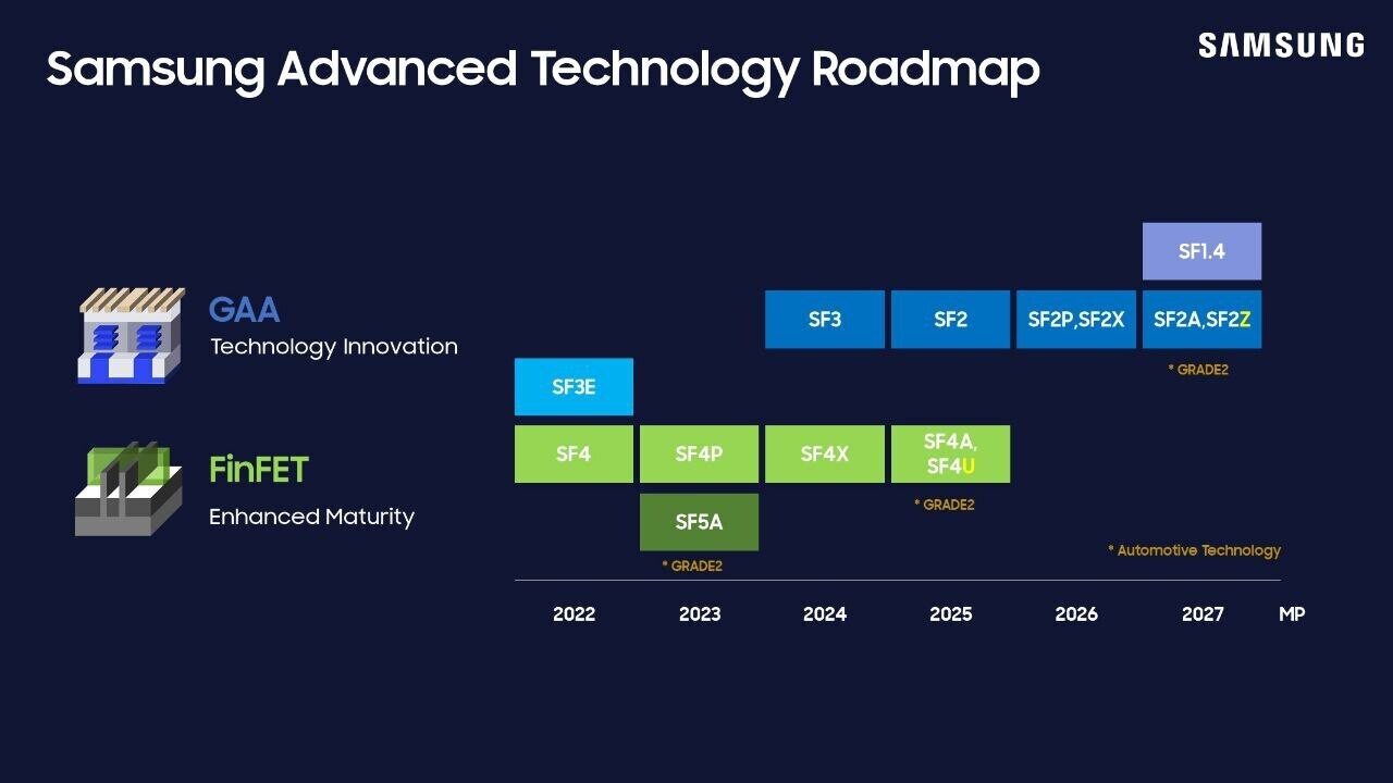
According to Wei, long-term agreements could include modest price increases, especially for advanced process nodes, where research and development costs and manufacturing challenges are rising. Looking ahead, TSMC confirmed that the upcoming A14 1.4 nm node wafers are expected to be priced around $45,000 each. This would represent a 50 percent increase over the current 2 nm wafers, which cost about $30,000 apiece. Production of the 1.4 nm node is projected to begin around 2028. Only TSMC's top-tier customers are likely to reserve capacity for this cutting-edge node in its early stages. As demand for advanced semiconductors rises, the company's approach to pricing and geographic focus will be key to maintaining its leadership in the global foundry market.

Insider Report Suggests Start of 1 nm Chip Development at Samsung, Alleged 2029 Mass Production Phase Targeted

Samsung's foundry business seems to be busying itself with the rumored refinement of a 2 nm GAA (SF2) manufacturing node process—for possible mass production by the end of 2025, but company leadership will very likely be considering longer term goals. Mid-way through last month, industry moles posited that the megacorporation's semiconductor branch was questioning the future of a further out 1.4 nm (SF1.4) production line. Officially published roadmaps have this advanced technology rolling out by 2027. Despite present day "turmoil," insiders believe that a new team has been established—tasked with the creation of a so-called "dream semiconductor process." According to a fresh Sedaily news article, this fledgling department has started development of a 1 nm foundry process.

Anonymous sources claim that Samsung executives are keeping a watchful eye on a main competitor—as stated in the latest South Korean report: "there is a realistic gap with Taiwan's TSMC in technologies that are close to mass production, such as the 2 nm process, the company plans to speed up the development of the 1 nm process, a future technology, to create an opportunity for a turnaround." A portion of the alleged "1 nm development chip team" reportedly consists of veteran researchers from prior-gen projects. Semiconductor industry watchdogs theorize that a canceled SF1.4 line could be replaced by an even more advanced process. Sedaily outlined necessary hardware upgrades: "the 1.0 nanometer process requires a new technology concept that breaks the mold of existing designs as well as the introduction of next-generation equipment such as high-NA EUV exposure equipment. The company is targeting mass production after 2029." Samsung's current Advanced Technology Roadmap does not extend beyond 2027—inside sources claim that the decision to roll with 1.0 nm was made at some point last month.

TSMC Reportedly Preparing New Equipment for 1.4 nm Trial Run at "P2" Baoshan Plant

Industry insiders posit that TSMC's two flagship fabrication facilities are running ahead of schedule with the development of an advanced 2 nm (N2) process node. A cross-facility mass production phase is tipped to begin later this year, which leaves room for next-level experiments. Taiwan's Economic Daily News has heard supply chain whispers about the Baoshan "P2" plant making internal preparations for a truly cutting edge 1.4 nm-class product. According to the report, unnamed sources have claimed that: "TSMC has made a major breakthrough in the advancement of its 1.4 nm process. (The company) has recently notified suppliers to prepare the necessary equipment for 1.4 nm, and plans to install a trial production 'mini-line' at P2 (Baoshan Fab 20)."

Their Hsinchu-adjacent "Fab 20" site is touted as a leading player in the prototyping of this new technology. Industry moles reckon that "1.4 nm expertise" will eventually trickle over to nearby "P3 and P4 plants" for full production phases. Allegedly, these factories were originally going to be involved in the manufacturing of 2 nm (N2) wafers. Additionally, TSMC's "Fab 25" campus could potentially play host to trial 1.4 nm activities—the Economic Daily News article proposes that four plants based in the Central Taiwan Science Park are pitching in with collaborative work. As interpreted by TrendForce, "P1" could begin "risk trial production" by 2027, followed by full-scale output within the following year.

Rapidus Set to Receive Japan's First ASML EUV Lithography Machine in December

The EUV lithography machine from ASML ordered by Rapidus is expected to arrive in Japan in mid-December, according to information from Nikkei cited by TrendForce. This marks the first deployment of EUV technology in Japan, an important step for the country's semiconductor industry as it seeks to establish itself as a major player. Rapidus is currently building a factory in Chitose, Hokkaido, and plans to start mass production of 2 nm chips in 2027. The company also plans to purchase several EUV devices if the 2-nanometer chip production is successful, and intends to build a second production facility specifically for 1.4 nm chips. To support these operations, ASML will establish a service center in Chitose City.

NVIDIA CEO Jensen Huang hinted at the possibility of outsourcing AI chip production to Rapidus. As of October, construction progress on the Rapidus facility, which began in September 2023, is up to 63% and remains on track. In addition to Rapidus, Micron's Hiroshima plant is scheduled to install EUV equipment in 2025, allowing for mass production in 2026. JASM, a TSMC subsidiary in Japan, plans to integrate EUV lithography with a second wafer plant in 2027 that will have a 6 nm production line.

Samsung to Launch 2nm Production Line with 7,000-Wafer Monthly Output by Q1 2025

Samsung Electronics is speeding up its work on 2 nm production facilities, industry sources say. The company has started to install advanced equipment at its "S3" foundry line in Hwaseong to set up a 2 nm production line. This line aims to produce 7,000 wafers each month by the first quarter of next year. Also, Samsung plans to create a 1.4 nm production line at its "S5" foundry in Pyeongtaek Plant 2 by the second quarter of next year. This line has a goal to make 2,000 to 3,000 wafers each month. By the end of next year, Samsung will change all the remaining 3 nm production lines at "S3" to 2 nm.

As we reported earlier, Samsung has pushed back the start date for its Tyler, Texas foundry. The plant set to open by late 2024, won't install equipment until after 2026. Also, Samsung has changed its plans for the Pyeongtaek Fab 4 foundry line. Because of lower demand, it will now make DRAM instead, moreover, at Pyeongtaek Fab 3, which has a 4 nm line, Samsung has cut back production. These changes are part of Samsung's plan to make 2 nm chips next year and 1.4 nm chips by 2027. The company wants to catch up with its rival TSMC, right now, Samsung has 11.5% of the global foundry market in Q2, while TSMC leads with 62.3%. An industry expert stressed how crucial this is saying, "With the delay in 3 nm Exynos production and other issues, getting the 2 nm process right could make or break Samsung Foundry". The struggle for Samsung is real, with the company's top management, led by DS Division Vice Chairman Jeon Young-hyun, having recently issued a public apology for the division's underwhelming performance.

Samsung Showcases AI-Era Vision and Latest Foundry Technologies at SFF 2024

Samsung Electronics, a world leader in advanced semiconductor technology, today unveiled its latest foundry innovations and outlined its vision for the AI era during Samsung Foundry Forum (SFF) U.S., an annual event held at the company's Device Solutions America headquarters in San Jose, California. Under the theme "Empowering the AI Revolution," Samsung announced its reinforced process technology roadmap, including two new cutting-edge nodes—SF2Z and SF4U—as well as its integrated Samsung AI Solutions platform harnessing the unique strengths of its Foundry, Memory and Advanced Package (AVP) businesses.

"At a time when numerous technologies are evolving around AI, the key to its implementation lies in high-performance, low-power semiconductors," said Dr. Siyoung Choi, President and Head of Foundry Business at Samsung Electronics. "Alongside our proven GAA process optimized for AI chips, we plan to introduce integrated, co-packaged optics (CPO) technology for high-speed, low-power data processing, providing our customers with the one-stop AI solutions they need to thrive in this transformative era."

Intel 14A Node Delivers 15% Improvement over 18A, A14-E Adds Another 5%

Intel is revamping its foundry play, and the company is set on its goals of becoming a strong contender to rivals such as TSMC and Samsung. Under Pat Gelsinger's lead, Intel recently split (virtually, under the same company) its units into Intel Product and Intel Foundry. During the SPIE 2024 conference for optics and photonics, Anne Kelleher, Intel's senior vice president, revealed that the 14A (1.4 nm) process offers a 15% performance-per-watt improvement over the company's 18A (1.8 nanometers) process. Additionally, the enhanced 14A-E process boasts a further 5% performance boost from the regular A14 node, being a small refresh. Intel's 14A process is set to be the first to utilize High-NA extreme ultraviolet (EUV) equipment, delivering a 20% increase in transistor logic density compared to the 18A node.

The company's aggressive pursuit of next-generation processes poses a significant threat to Samsung Electronics, which currently holds the second position in the foundry market. As part of its IDM 2.0 strategy, Intel hopes to reclaim its position as a leading foundry player and surpass Samsung by 2030. The company's collaboration with American companies, such as Microsoft, further solidifies its ambitions. Intel has already secured a $15 billion chip production contract with Microsoft for its 1.8 nm 18A process. The semiconductor industry is closely monitoring Intel's progress, as the company's advancements in process technology could potentially reshape the competitive landscape. With Samsung planning to mass-produce 2 nm process products next year, the race for dominance in the foundry market is heating up.

TSMC Allegedly Not Rushing into Adoption of High-NA EUV Machinery

DigiTimes Asia has reached out to insiders at fabrication toolmakers in an effort to delve deeper into claims made by industry analysts at the start of 2024—both SemiAnalysis and China Renaissance have proposed that TSMC is unlikely to adopt High-NA EUV production techniques within a five year period. The latest news article explores a non-upgrade approach for the next couple of years: "TSMC has not placed orders for high-numerical aperture (High-NA) extreme ultraviolet (EUV) tools and is unlikely to use the technology in 2 nm and 1.4 nm (A14) process manufacturing." Intel Foundry Services (IFS) will be one of the first semiconductor manufacturers to go online with ASML's latest and greatest machinery, although no firm timeframes have been confirmed. Team Blue's Taiwanese rival (and occasional business partner) is seemingly happy with its existing infrastructure, but industry watchdogs propose that cost considerations are key factors behind TSMC's cautious planning for the next decade.

The DigiTimes insider sources believe that TSMC will not budge until at least 2029, possibly coinciding with a 1 nm production node—analysts at China Renaissance reckon that High-NA EUV machines could be delivered in the future when facilities are readied for an "A10" codenamed process. TSMC published a very ambitious "transistor count" product timeline in early January (see below)—the first "1 nm" products are supposedly targeted for a 2030 rollout, but this schedule could change due to unforeseen circumstances. Intel is expected to "phase in" its fanciest ASML gear collection once the 18A process becomes old hat—Tom's Hardware thinks that 2026 - 2027 is a feasible timeframe.

TSMC Said to Start Construction of 1.4 nm Fab in 2026

According to Taiwanese media, TSMC will start production of its first 1.4 nm fab in 2026, with chip production in the fab said to start sometime in 2027 or 2028. The new fab will be located in Longtan Science Park outside of Hsinchu in Taiwan, where many of TSMC's current fabs are located. TSMC is currently constructing a 2 nm and below node R&D facility at a nearby plot of land to where the new fab is expected to be built. This facility is expected to be finished in 2025 and TSMC has been allocated a total area of just over 158 hectares of land for future expansion in the area.

In related news, TSMC is expected to be charging US$25,000 per 2 nm GAA wafer, which is an increase of about a fifth compared to its 3 nm wafers which are going for around US$20,000. This is largely due to the nodes being fully booked and TSMC being able to charge a premium for its cutting edge nodes. TSMC is also expanding in CoWoS packaging facilities due to increased demand from both AMD and NVIDIA for AI related products. Currently TSMC is said to be able to output 12,000 CoWoS wafers per month and this is twice as much as last year, yet TSMC is unable to meet demand from its customers.

TSMC N1 Node Chip Plant Said to be Under Planning

Based on news out of Taiwan, TSMC is said to be in the early planning stages of yet another chip plant, this time for its first N1 node. The new plant will reportedly be built in a science park in Taoyuan, less than an hour south west of Taipei, according to the Commercial Times. TSMC already has a pair of chip packaging and testing facilities in the science park, making it a suitable location for a chip plant. This will be TSMC's most northern chip manufacturing plant in Taiwan, although it's not expected to start pilot production until sometime in 2027. TSMC hasn't confirmed any of the details, but the company didn't outright deny the report either.

Despite the potential global downturn in the economy, TSMC appears to be fully committed to continue to build new fabs for increasingly smaller nodes. The company is set to start its first commercial production on its N3 node this quarter and is expecting the N3 node to contribute as much as four to six percent of its overall revenue in 2023. Its N2 node should enter commercial production in 2025, but not much is known about the state of the N2 node at this point in time. The N1 node might end up being a 1.4 nm node, based on TSMC's measurements, but the company is still in the very beginning of the R&D phase for this node.

Samsung Electronics Unveils Plans for 1.4 nm Process Technology

Samsung Electronics, a world leader in advanced semiconductor technology, announced today a strengthened business strategy for its Foundry Business with the introduction of cutting-edge technologies at its annual Samsung Foundry Forum event. With significant market growth in high-performance computing (HPC), artificial intelligence (AI), 5/6G connectivity and automotive applications, demand for advanced semiconductors has increased dramatically, making innovation in semiconductor process technology critical to the business success of foundry customers. To that end, Samsung highlighted its commitment to bringing its most advanced process technology, 1.4-nanometer (nm), for mass production in 2027.

During the event, Samsung also outlined steps its Foundry Business is taking in order to meet customers' needs, including: foundry process technology innovation, process technology optimization for each specific applications, stable production capabilities, and customized services for customers. "The technology development goal down to 1.4 nm and foundry platforms specialized for each application, together with stable supply through consistent investment are all part of Samsung's strategies to secure customers' trust and support their success," said Dr. Si-young Choi, president and head of Foundry Business at Samsung Electronics. "Realizing every customer's innovations with our partners has been at the core of our foundry service."
Return to Keyword Browsing
Jul 14th, 2025 15:42 CDT change timezone

New Forum Posts

Popular Reviews

TPU on YouTube

Controversial News Posts