News Posts matching #7 nm+

Return to Keyword Browsing

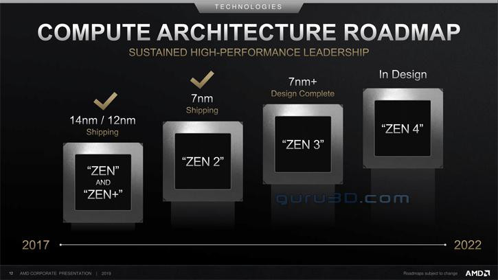
AMD 32-Core EPYC "Milan" Zen 3 CPU Fights Dual Xeon 28-Core Processors

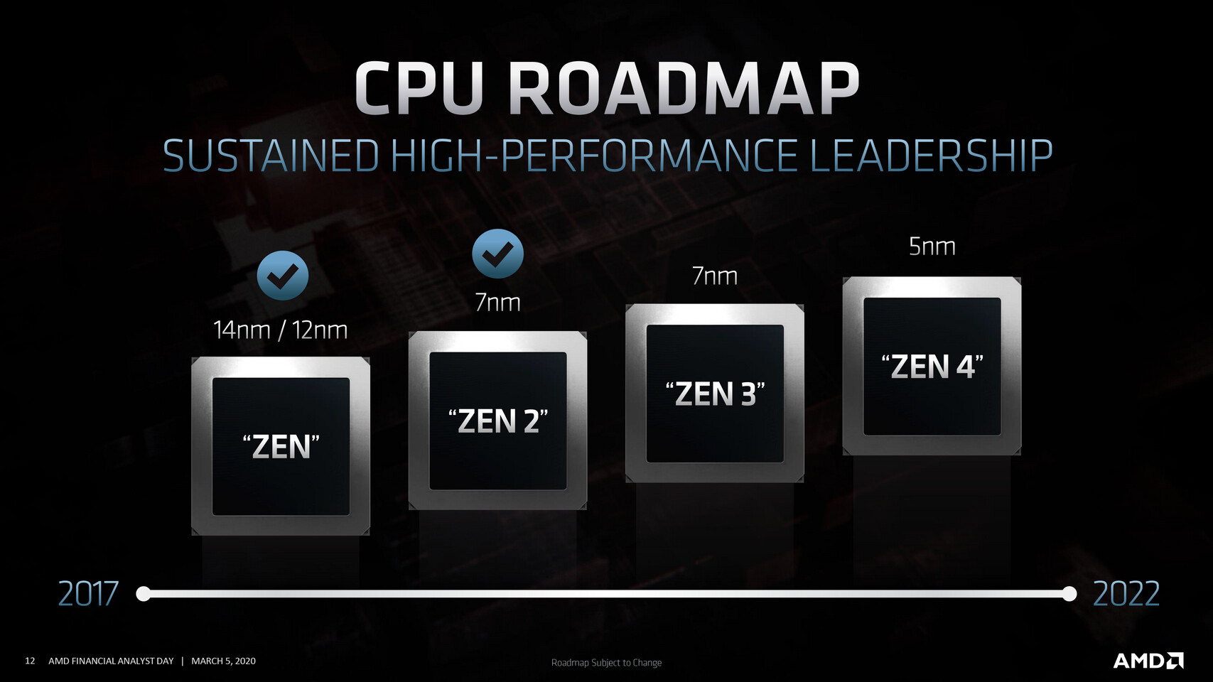
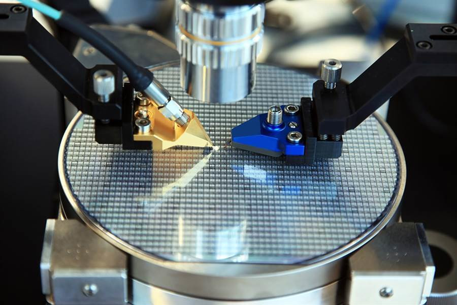
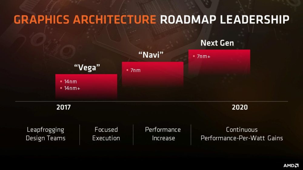
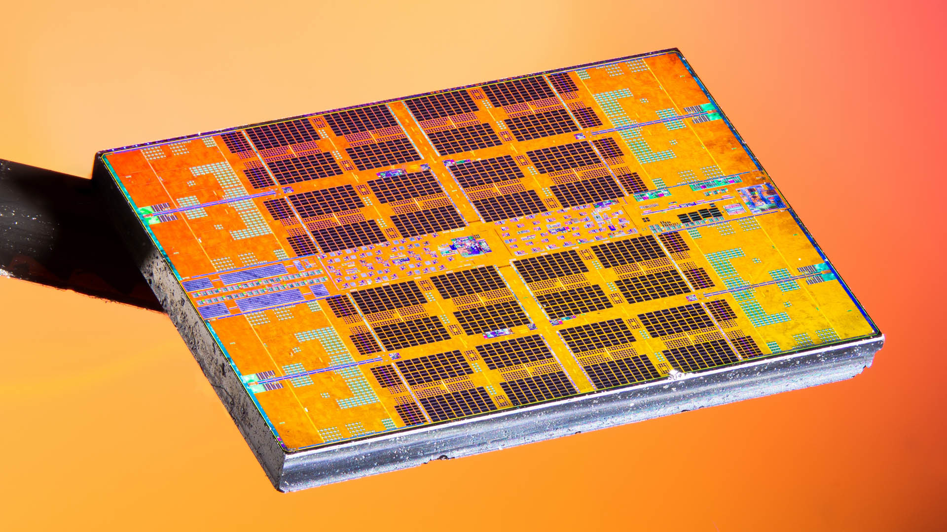
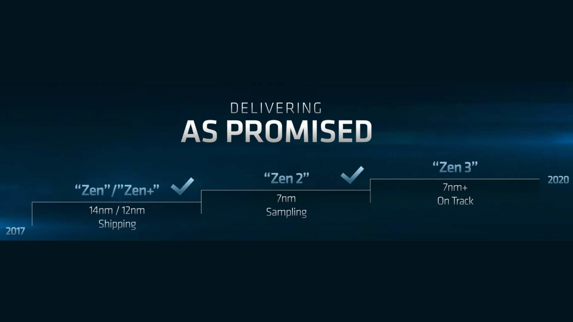
AMD is expected to announce its upcoming EPYC lineup of processors for server applications based on the new Zen 3 architecture. Codenamed "Milan", AMD is continuing the use of Italian cities as codenames for its processors. Being based on the new Zen 3 core, Milan is expected to bring big improvements over the existing EPYC "Rome" design. Bringing a refined 7 nm+ process, the new EPYC Milan CPUs are going to feature better frequencies, which are getting paired with high core counts. If you are wondering how Zen 3 would look like in server configuration, look no further because we have the upcoming AMD EPYC 7543 32-core processor benchmarked in Geekbench 4 benchmark.

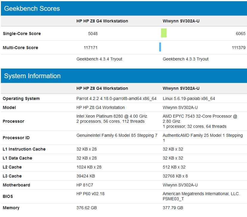
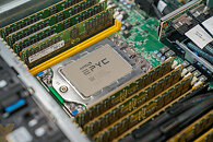
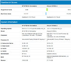
The new EPYC 7543 CPU is a 32 core, 64 thread design with a base clock of 2.8 GHz, and a boost frequency of 3.7 GHz. The caches on this CPU are big, and there is a total of 2048 KB (32 times 32 KB for instruction cache and 32 times 32 KB for data cache) of L1 cache, 16 MB of L2 cache, and as much as 256 MB of L3. In the GB4 test, a single-core test produced 6065 points, while the multi-core run resulted in 111379 points. If you are wondering how that fairs against something like top-end Intel Xeon Platinum 8280 Cascade Lake 28-core CPU, the new EPYC Milan 7543 CPU is capable of fighting two of them at the same time. In a single-core test, the Intel Xeon configuration scores 5048 points, showing that the new Milan CPU has 20% higher single-core performance, while the multi-core score of the dual Xeon setup is 117171 points, which is 5% faster than AMD CPU. The reason for the higher multi-core score is the sheer number of cores that a dual-CPU configuration offers (32 cores vs 56 cores).

First Signs of AMD Zen 3 "Vermeer" CPUs Surface, Ryzen 7 5800X Tested

AMD is preparing to launch the new iteration of desktop CPUs based on the latest Zen 3 core, codenamed Vermeer. On October 8th, AMD will hold the presentation and again deliver the latest technological advancements to its desktop platform. The latest generation of CPUs will be branded as a part of 5000 series, bypassing the 4000 series naming scheme which should follow, given that the prior generation was labeled as 3000 series of processors. Nonetheless, AMD is going to bring a new Zen 3 core with its processors, which should bring modest IPC gains. It will be manufactured on TSMC's 7 nm+ manufacturing node, which offers a further improvement to power efficiency and transistor density.

Today, we have gotten the first benchmark of AMD's upcoming Ryzen 7 5800X CPU. Thanks to the popular hardware leaker, TUP APISAK, we have the first benchmark of the new Vermeer processor, compared to Intel's latest and greatest - Core i9-10900K. The AMD processor is an eight-core, sixteen threaded model compared to the 10C/20T Intel processor. While we do not know the final clocks of the AMD CPU, we could assume that the engineering sample was used and we could see an even higher performance. Below you can see the performance of the CPU and how it compares to Intel. By the numbers shown, we can expect AMD to possibly be a new gaming king, as the numbers are very close to Intel. The average batch result for the Ryzen 7 5800X was 59.3 FPS and when it comes to CPU frames it managed to score 133.6 FPS. Intel's best managed to average 60.3 FPS and 114.8 FPS from the CPU framerates. Both systems were tested with NVIDIA's GeForce RTX 2080 GPUs.

TSMC Owns 50% of All EUV Machines and Has 60% of All EUV Wafer Capacity

TSMC had been working super hard in the past few years and has been investing in lots of new technologies to drive the innovation forward. At TSMC's Technology Symposium held this week was, the company has presented various things like the update on its 12 nm node, as well as future plans for node development. One of the most interesting announcements made this week was TSMC's state and ownership of Extreme Ultra-Violet (EUV) machines. ASML, the maker of these EUV machines used to etch the pattern on silicon, has been the supplier of the Taiwanese company. TSMC has announced that they own an amazing 50% of all EUV machine installations.

What is more important is the capacity that the company achieves with it. It is reported that TSMC achieves 60% of all EUV wafer capacity in the world, which is a massive achievement of what TSMC can do with the equipment. The company right now has only two nodes on EUV in high-volume manufacturing, the 7 nm+ node and 5 nm node (which is going HVM in Q4), however, that is more than any of its competitors. All of the future nodes are to be manufactured using the EUV machines and the smaller nodes require it. As far as the competitors go, only Samsung is currently making EUV silicon on the 7 nm LPP node. Intel is yet to release some products on a 7 nm node of its own, which is the first EUV node from the company.

AMD Sheds Light on the Missing "+" in "7nm" for Zen 3 and RDNA2 in its Latest Presentation

AMD at its Financial Analyst Day 2020 presentation made a major clarification about its silicon fabrication process. It was previously believed that the company's upcoming "Zen 3" CPU microarchitecture and RDNA2 graphics architectures were based on TSMC's N7+ (7 nm EUV) silicon fabrication process because AMD would mark the two as "7 nm+" in its marketing slides. Throughout its Financial Analyst Day presentation, however, AMD avoided using that marker, and resorted to an amorphous "7 nm" marker, prompting one of the financial analysts to seek a clarification. At the time, AMD responded that they were aligning their marketing with that of TSMC, and hence chose to use "7 nm" in its new slides.

It turns out that the next step to TSMC N7, the company's current-generation 7 nm DUV silicon fabrication node, isn't N7+ (7 nm EUV), but rather it has a nodelet along the way, which the foundry refers to as N7P. This is a generational refinement of N7, but does not use EUV lithography, which means it may not offer the 15-20 percent gains in transistor densities offered by N7+ over N7. AMD clarified that "7 nm+" in its past presentations did not intend to signify N7+, and that the "+" merely denoted an improvement over N7. At the same time, it won't specify whether "Zen 3" and RDNA2 are based on N7P or N7+, so the company doesn't rule out N7+, either. We'll probably learn more as we near the late-2020 launch of "Zen 3" as EPYC "Milan."
AMD CPU Roadmap Zen 3 Zen 4 AMD CPU Roadmap Zen 2 Zen 3

AMD RDNA2 Graphics Architecture Detailed, Offers +50% Perf-per-Watt over RDNA

With its 7 nm RDNA architecture that debuted in July 2019, AMD achieved a nearly 50% gain in performance/Watt over the previous "Vega" architecture. At its 2020 Financial Analyst Day event, AMD made a big disclosure: that its upcoming RDNA2 architecture will offer a similar 50% performance/Watt jump over RDNA. The new RDNA2 graphics architecture is expected to leverage 7 nm+ (7 nm EUV), which offers up to 18% transistor-density increase over 7 nm DUV, among other process-level improvements. AMD could tap into this to increase price-performance by serving up more compute units at existing price-points, running at higher clock speeds.

AMD has two key design goals with RDNA2 that helps it close the feature-set gap with NVIDIA: real-time ray-tracing, and variable-rate shading, both of which have been standardized by Microsoft under DirectX 12 DXR and VRS APIs. AMD announced that RDNA2 will feature dedicated ray-tracing hardware on die. On the software side, the hardware will leverage industry-standard DXR 1.1 API. The company is supplying RDNA2 to next-generation game console manufacturers such as Sony and Microsoft, so it's highly likely that AMD's approach to standardized ray-tracing will have more takers than NVIDIA's RTX ecosystem that tops up DXR feature-sets with its own RTX feature-set.
AMD GPU Architecture Roadmap RDNA2 RDNA3 AMD RDNA2 Efficiency Roadmap AMD RDNA2 Performance per Watt AMD RDNA2 Raytracing

AMD Announces the CDNA and CDNA2 Compute GPU Architectures

AMD at its 2020 Financial Analyst Day event unveiled its upcoming CDNA GPU-based compute accelerator architecture. CDNA will complement the company's graphics-oriented RDNA architecture. While RDNA powers the company's Radeon Pro and Radeon RX client- and enterprise graphics products, CDNA will power compute accelerators such as Radeon Instinct, etc. AMD is having to fork its graphics IP to RDNA and CDNA due to what it described as market-based product differentiation.

Data centers and HPCs using Radeon Instinct accelerators have no use for the GPU's actual graphics rendering capabilities. And so, at a silicon level, AMD is removing the raster graphics hardware, the display and multimedia engines, and other associated components that otherwise take up significant amounts of die area. In their place, AMD is adding fixed-function tensor compute hardware, similar to the tensor cores on certain NVIDIA GPUs.
AMD Datacenter GPU Roadmap CDNA CDNA2 AMD CDNA Architecture AMD Exascale Supercomputer

AMD to Debut 2nd Gen RDNA Architecture in 2020

AMD CEO Dr Lisa Su, in her Q4-2019 and FY-2019 earnings call, confirmed that the company debut its second-generation RDNA graphics architecture in 2020. "In 2019 we launched our new architecture in GPUs, it's the RDNA architecture, and that was the Navi-based products. You should expect those will be refreshed in 2020, and we will have our new next-generation RDNA architecture that will be part our 2020 lineup."

Second-gen RDNA, or RDNA2, is expected to leverage the new 7 nm+ (EUV) silicon fabrication process at TSMC, to dial up transistor-counts, clock-speeds, and performance. Among the two anticipated feature additions are VRS (variable rate shading) and possibly ray-tracing. The fabled "big Navi" silicon, a GPU larger than "Navi 10," is also on the cards, according to an earlier statement by Dr Su. More details about these upcoming graphics cards are expected to be put out in March, at the 2020 AMD Investor Day conference.

Expect High-end Navi: AMD CEO

At a Q&A session with the tech press in Las Vegas, AMD CEO Dr Lisa Su raised hopes of a high-end graphics card based on its "Navi" family of GPUs. Responding to a specific question by Gordon Ung from PC World on whether there will be a high-end competitor in the discrete graphics space, Dr Su stated that one should expect a "high-end Navi." Dr Su states: "I know those on Reddit want a high end Navi! You should expect that we will have a high-end Navi, and that it is important to have it. The discrete graphics market, especially at the high end, is very important to us. So you should expect that we will have a high-end Navi, although I don't usually comment on unannounced products."

For months now, it's been speculated that AMD has been working on a larger GPU die than "Navi 10." In 2020, AMD is expected to release the "Navi 20" familly of GPUs built on 7 nm+ (EUV) node, based on the RDNA2 graphics architecture. The key design goals of RDNA2 are expected to be support for at least tier-1 variable-rate shading (VRS), and possibly hardware-accelerated ray-tracing. It's possible that "high-end Navi" belongs to this family of GPUs.

AMD to Outpace Apple as TSMC's Biggest 7nm Customer in 2020

AMD in the second half of 2020 could outpace Apple as the biggest foundry customer of TSMC for its 7 nm silicon fabrication nodes (DUV and EUV combined). There are two key factors contributing to this: AMD significantly increasing its orders for the year; and Apple transitioning to TSMC's 5 nm node for its A14 SoC, freeing up some 7 nm allocation, which AMD grabbed. AMD is currently tapping into 7 nm DUV for its "Zen 2" chiplet, "Navi 10," and "Navi 14" GPU dies. The company could continue to order 7 nm DUV until these products reach EOL; while also introducing the new "Renoir" APU die on the process. The foundry's new 7 nm+ (EUV) node will be utilized for "Zen 3" chiplets and "Navi 2#" GPU dies in 2020.

Currently, the top-5 customers for TSMC 7 nm are Apple, HiSilicon, Qualcomm, AMD, and MediaTek. Barring AMD, the others in the top-5 build mobile SoCs or 4G/5G modem chips on the node. AMD is expected to top the list as it scales up orders with TSMC. In the first half of 2020, TSMC's monthly output for 7 nm is expected to grow to 110,000 wafers per month (wpm). Apple's migration to 5 nm in 2H-2020, coupled with capacity-addition could take TSMC's 7 nm output to 140,000 wpm. AMD has reportedly booked the entire capacity-addition for 30,000 wpm, taking its allocation up to 21% in 2H-2020. Qualcomm is switching to Samsung for its next-generation SoCs and modems designed for 7 nm EUV. NVIDIA, too, is expected to built its next-gen 7 nm EUV GPUs on Samsung instead of TSMC. These moves by big players could free up significant foundry allocation at TSMC for AMD's volumes to grow in 2020.

AMD "Zen 4" 2021 Launch On Track as TSMC Optimistic About 5 nm

AMD's "Zen 4" CPU microarchitecture is on track for a 2021 launch as its principal foundry partner, TSMC, is optimistic about early yields of its 5 nm silicon fabrication node. TSMC supports the 5 nm product roadmaps of not just AMD, but also Apple and HiSilicon. "Zen 4" is particularly important for AMD, as it will release its next enterprise platform, codenamed "Genoa," along with the new SP5 socket. The new socket will present AMD with the opportunity to significantly change the processor's I/O, such as support for a new memory standard, a new PCIe generation, more memory channels, more PCIe lanes, etc. As early as 2019, the foundry is seeing yields of over 50 percent for the 5 nm node (possibly risk production designed to test the node), which is very encouraging for its customers.

AMD's roadmap for 2020 sees the introduction of "Zen 3" on the 7 nm EUV process (dubbed 7 nm+). AMD recently commented that the performance uplift of "Zen 3" versus "Zen 2" will be "right in line with what you would expect from an entirely new architecture." The 7 nm EUV node provides a significant 20 percent increase in transistor-density compared to the current 7 nm DUV node "Zen 2" chiplets and the company's "Navi" family of GPUs are built on. "Zen 3" could see the company do away with the CCX (quad-core CPU complex), and make chiplets monolithic blocks of CPU cores without sub-divisions. For the client-segment, 5 is a recurring number in 2021. It will see the introduction of the 5th generation Ryzen processors (5000-series), built on the 5 nm process, supporting DDR5 memory, PCI-Express gen 5, and the new AM5 client-segment CPU socket.

AMD Could Launch Next Generation RDNA 2 GPUs at CES 2020

According to the findings of a Chiphell user called "wjm47196", AMD is supposedly going to host an event at CES 2020 to showcase its next generation of Radeon graphics cards. Having seen huge success with its first-generation "RDNA" GPUs, AMD is expected to showcase improved lineup utilizing new and improved RDNA 2 graphics card architecture.

Judging by the previous information, second generation of RDNA graphics cards will get much-needed features like ray tracing, to remain competitive with existing offers from NVIDIA and soon Intel. Supposed to be built using the 7 nm+ manufacturing process, the new GPU architecture will get around 10-15% performance improvement due to the new manufacturing process alone, with possibly higher numbers if there are changes to the GPU core.

TSMC Trembles Under 7 nm Product Orders, Increases Delivery Lead Times Threefold - Could Hit AMD Product Availability

TSMC is on the vanguard of chipset fabrication technology at this exact point in time - its 7 nm technology is the leading-edge of all large volume processes, and is being tapped by a number of companies for 7 nm silicon. One of its most relevant clients for our purposes, of course, is AMD - the company now enjoys a fabrication process lead over arch-rival Intel much due to its strategy of fabrication spin-off and becoming a fabless designer of chips. AMD's current product stack has made waves in the market by taking advantage of 7 nm's benefits, but it seems this may actually become a slight problem in the not so distant future.

TSMC has announced a threefold increase in its delivery lead times for 7 nm orders, from two months to nearly six months, which means that orders will now have to wait three times longer to be fulfilled than they once did. This means that current channel supplies and orders made after the decision from TSMC will take longer to materialize in actual silicon, which may lead to availability slumps should demand increase or maintain. AMD has its entire modern product stack built under the 7 nm process, so this could potentially affect both CPUs and GPUs from the company - and let's not forget AMD's Zen 3 and next-gen RDNA GPUs which are all being designed for the 7 nm+ process node. TSMC is expected to set aside further budget to expand capacity of its most advanced nodes, whilst accelerating investment on their N7+, N6, N5, and N3 nodes.

AMD Updates Roadmaps to Lock RDNA2 and Zen 3 onto 7nm+, with 2020 Launch Window

AMD updated its technology roadmaps to reflect a 2020 launch window for its upcoming CPU and graphics architectures, "Zen 3" and RDNA2. The two will be based on 7 nm+ , which is AMD-speak for the 7 nanometer EUV silicon fabrication process at TSMC, that promises a significant 20 percent increase in transistor-densities, giving AMD high transistor budgets and more clock-speed headroom. The roadmap slides however hint that unlike the "Zen 2" and RDNA simultaneous launch on 7th July 2019, the next-generation launches may not be simultaneous.

The slide for CPU microarchitecture states that the design phase of "Zen 3" is complete, and that the microarchitecture team has already moved on to develop "Zen 4." This means AMD is now developing products that implement "Zen 3." On the other hand, RDNA2 is still in design phase. The crude x-axis on both slides that denotes year of expected shipping, too appears to suggest that "Zen 3" based products will precede RDNA2 based ones. "Zen 3" will be AMD's first response to Intel's "Comet Lake-S" or even "Ice Lake-S," if the latter comes to fruition before Computex 2020. In the run up to RDNA2, AMD will scale up RDNA a notch larger with the "Navi 12" silicon to compete with graphics cards based on NVIDIA's "TU104" silicon. "Zen 2" will receive product stack additions in the form of a new 16-core Ryzen 9-series chip later this month, and the 3rd generation Ryzen Threadripper family.

Intel "Sapphire Rapids" Brings PCIe Gen 5 and DDR5 to the Data-Center

As if the mother of all ironies, prior to its effective death-sentence dealt by the U.S. Department of Commerce, Huawei's server business developed an ambitious product roadmap for its Fusion Server family, aligning with Intel's enterprise processor roadmap. It describes in great detail the key features of these processors, such as core-counts, platform, and I/O. The "Sapphire Rapids" processor will introduce the biggest I/O advancements in close to a decade, when it releases sometime in 2021.

With an unannounced CPU core-count, the "Sapphire Rapids-SP" processor will introduce DDR5 memory support to the data-center, which aims to double bandwidth and memory capacity over the DDR4 generation. The processor features an 8-channel (512-bit wide) DDR5 memory interface. The second major I/O introduction is PCI-Express gen 5.0, which not only doubles bandwidth over gen 4.0 to 32 Gbps per lane, but also comes with a constellation of data-center-relevant features that Intel is pushing out in advance as part of the CXL Interconnect. CXL and PCIe gen 5 are practically identical.

Intel Switches Gears to 7nm Post 10nm, First Node Live in 2021

Intel's semiconductor manufacturing business has had a terrible past 5 years as it struggled to execute its 10 nanometer roadmap forcing the company's processor designers to re-hash the "Skylake" microarchitecture for 5 generations of Core processors, including the upcoming "Comet Lake." Its truly next-generation microarchitecture, codenamed "Ice Lake," which features a new CPU core design called "Sunny Cove," comes out toward the end of 2019, with desktop rollouts expected 2020. It turns out that the 10 nm process it's designed for, will have a rather short reign at Intel's fabs. Speaking at an investor's summit on Wednesday, Intel put out its silicon fabrication roadmap that sees an accelerated roll-out of Intel's own 7 nm process.

When it goes live and fit for mass production some time in 2021, Intel's 7 nm process will be a staggering 3 years behind TSMC, which fired up its 7 nm node in 2018. AMD is already mass-producing CPUs and GPUs on this node. Unlike TSMC, Intel will implement EUV (extreme ultraviolet) lithography straightaway. TSMC began 7 nm with DUV (deep ultraviolet) in 2018, and its EUV node went live in March. Samsung's 7 nm EUV node went up last October. Intel's roadmap doesn't show a leap from its current 10 nm node to 7 nm EUV, though. Intel will refine the 10 nm node to squeeze out energy-efficiency, with a refreshed 10 nm+ node that goes live some time in 2020.

AMD Zen3 to Leverage 7nm+ EUV For 20% Transistor Density Increase

AMD "Zen 3" microarchitecture could be designed for the enhanced 7 nm+ EUV (extreme ultraviolet) silicon fabrication node at TSMC, which promises a significant 20 percent increase in transistor densities compared to the 7 nm DUV (deep ultraviolet) node on which its "Zen 2" processors are being built. In addition, the node will also reduce power consumption by up to 10 percent at the same operational load. In a late-2018 interview, CTO Mark Papermaster stated AMD's design goal with "Zen 3" would be to prioritize energy-efficiency, and that it would present "modest" performance improvements (read: IPC improvements) over "Zen 2." AMD made it clear that it won't drag 7 nm DUV over more than one microarchitecture (Zen 2), and that "Zen 3" will debut in 2020 on 7 nm+ EUV.

AMD "Navi" GPU Architecture Successor Codenamed "Arcturus"?

Arcturus is the fourth brightest star in the night sky, and could be the a new GPU architecture by AMD succeeding "Navi," according to a Phoronix report. The codename of Navi-successor has long eluded AMD's roadmap slides. The name "Arcturis" surfaced on Phoronix community forums, from a post by an AMD Linux liaison who is a member there. The codename is also supported by the fact that AMD is naming its GPU architectures after the brightest stars in the sky (albeit in a descending order of their brightness). Polaris is the brightest, followed by Vega, Navi, and Arcturus.

AMD last referenced the Navi-successor on a roadmap slide during its 2017 Financial Analyst Day presentation by Mark Papermaster. That slide mentioned "Vega" to be built on two silicon fabrication processes, 14 nm and "14 nm+." We know now that AMD intends to build a better-endowed "Vega" chip on 7 nm, which could be the world's first 7 nm GPU. "Navi" is slated to be built on 7 nm as the process becomes more prevalent in the industry. The same slide mentions Navi-successor as being built on "7 nm+," which going by convention, could refer to an even more advanced process than 7 nm. Unfortunately, even in 2017, when the industry was a touch more optimistic about 7 nm, AMD expected the Navi-successor to only come out by 2020. We're not holding our breath.

Analyst Firm Susquehanna: "Intel Lost its Manufacturing Leadership"

Intel was once the shining star in the semiconductor manufacturing industry, with a perfectly integrated, vertical product design and manufacturing scheme. Intel was one of the few companies in the world to be able to both develop its architectures and gear their manufacturing facilities to their design characteristics, ensuring a perfect marriage of design and manufacturing. However, not all is rosy on that field, as we've seen; AMD itself also was a fully integrated company, but decided to spin-off its manufacturing arm so as to survive - thus creating GLOBALFOUNDRIES.But Intel was seen as many as the leader in semiconductor manufacturing, always at the cutting edge of - well - Moore's Law, named after Intel's founding father Gordon Moore. Now, Mehdi Hosseini, an analyst with Susquehanna, has gone on to say that the blue giant has effectively lost its semiconductor leadership. And it has, in a way, even if its 10 nm (which is in development hell, so to speak) is technically more advanced than some 7 nm implementations waiting to be delivered to market by its competitors. However, there's one area where Intel will stop being able to claim leadership: manufacturing techniques involving EUV (Extreme UltraViolet).

TSMC to Bring 3D Stacked Wafers to Complex Silicon Designs, Such as GPUs

TSMC is close to adapt 3D stacked silicon wafers to complex silicon designs, such as graphics processors, using its new proprietary Wafer-on-Wafer (WoW) Advanced Packaging technology, which will be introduced with its 7 nm+ and 5 nm nodes. 3D stacked silicon fabrication is currently only implemented on "less complex" silicon designs, such as NAND flash, which don't run anywhere near as hot as complex designs ASIC designs, such as GPUs or CPUs. In its current form, TSMC achieved 2-layer stacks, in which two silicon layers that are "mirror images" of each other (for perfect alignment), sandwich bonding layers, through which pins for the upper layer pass through.

The bonding of the two layers is where the bulk of TSMC's innovations and "secret sauces" lie. For 3D NAND flash, multiple pancaked dies are wired out through their edges. You don't need as many pins to talk to a NAND flash die, as say a GPU die. For complex dies, designers have to pass thousands of pins through the "bottom layer," the connecting substrate, and eventually to the "top layer." The bottom layer hence is bumped out on both ends, one side interfacing with the package substrate for both dies, and the top side serving as a sort of substrate for the top die. This innovation is what TSMC calls "thru-silicon-vias" or TSVs.

AMD Reveals CPU, Graphics 2018-2020 Roadmap at CES

AMD at CES shed some light on its 2018 roadmap, while taking the opportunity to further shed some light on its graphics and CPU projects up to 2020. Part of their 2018 roadmap was the company's already announced, across the board price-cuts for their first generation Ryzen processors. This move aims to increase competitiveness of its CPU offerings against rival Intel - thus taking advantage of the blue giant's currently weakened position due to the exploit saga we've been covering. This move should also enable inventory clearings of first-gen Ryzen processors - soon to be supplanted by the new Zen+ 12 nm offerings, which are expected to receive a 10% boost to power efficiency from the process shrink alone, while also including some specific improvements in optimizing their performance per watt profile. These are further bound to see their market introduction in March, and are already in the process of sampling.

On the CPU side, AMD's 2018 roadmap further points towards a Threadripper and Ryzen Pro refresh in the 2H 2018, likely in the same vein as their consumer CPUs that we just talked about. On the graphics side of their 2018 roadmap, AMD focused user's attention in the introduction of premium Vega offerings in the mobile space (with HBM2 memory integration on interposer, as well), which should enable the company to compete against NVIDIA in the discrete graphics space for mobile computers. Another very interesting tidbit announced by AMD is that they would be skipping the 12 nm process for their graphics products entirely; the company announced that it will begin sampling of 7 nm Vega products to its partners, but only on the Instinct product line of machine learning accelerators. We consumers will likely have to wait a little while longer until we see some 7 nm graphics cards from AMD.
Return to Keyword Browsing
May 4th, 2024 04:13 EDT change timezone

New Forum Posts

Popular Reviews

Controversial News Posts