News Posts matching #Flash Memory

Return to Keyword Browsing

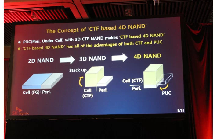
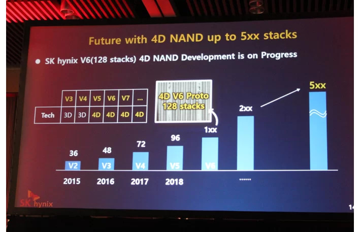
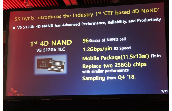
Kioxia and Western Digital Announce 6th-Generation 162-layer 3D NAND Flash Memory

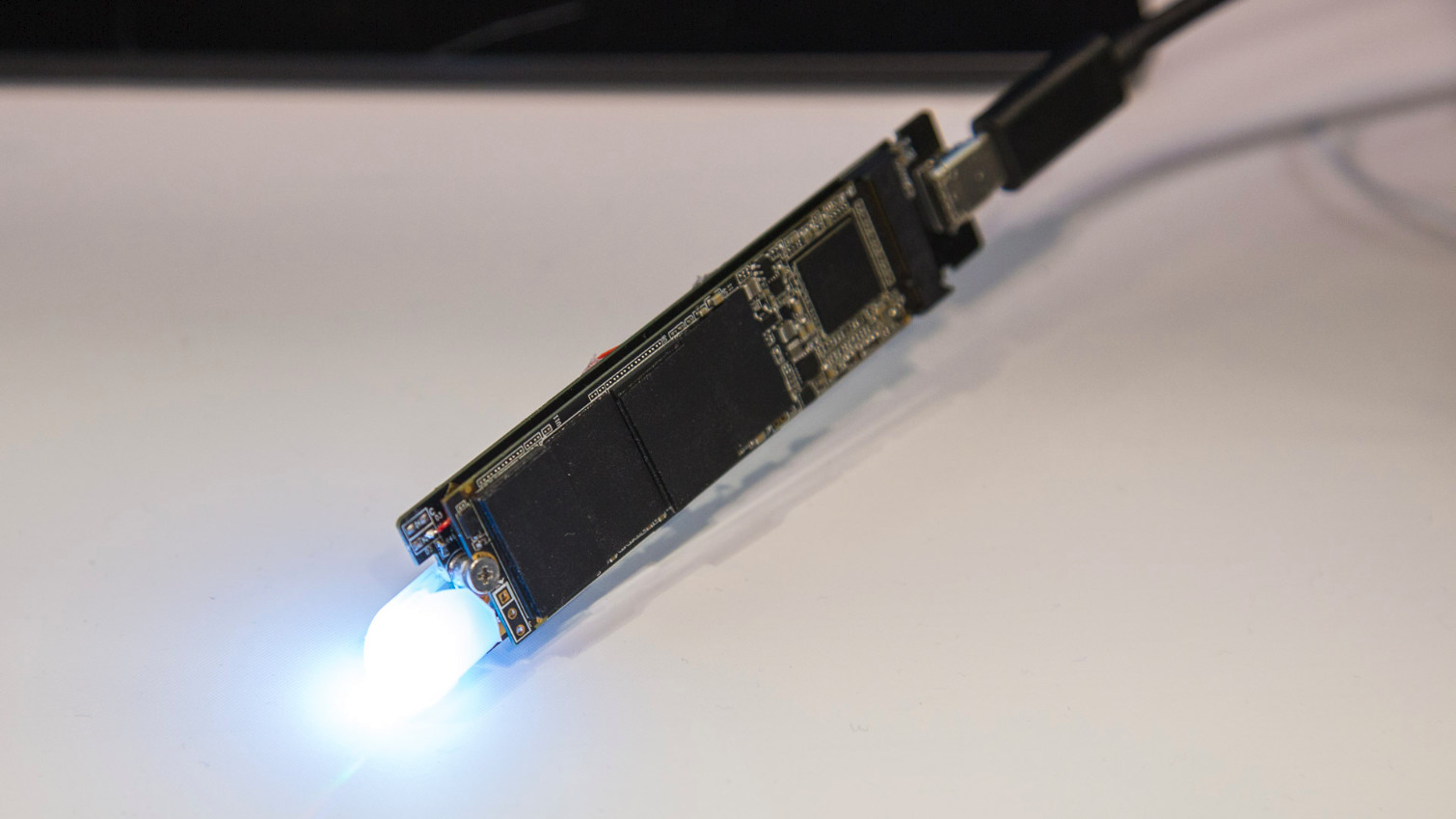
Kioxia Corporation and Western Digital Corp., today announced that the companies have developed their sixth-generation, 162-layer 3D flash memory technology. Marking the next milestone in the companies' 20-year joint-venture partnership, this is the companies' highest density and most advanced 3D flash memory technology to date, utilizing a wide range of technology and manufacturing innovations.

"Through our strong partnership that has spanned two decades, Kioxia and Western Digital have successfully created unrivaled capabilities in manufacturing and R&D," said Masaki Momodomi, Chief Technology Officer, Kioxia. "Together, we produce over 30 percent of the world's flash memory bits and are steadfast in our mission to provide exceptional capacity, performance and reliability at a compelling cost. We each deliver this value proposition across a range of data-centric applications from personal electronics to data centers as well as emerging applications enabled by 5G networks, artificial intelligence and autonomous systems."

PNY Announces 1TB PRO Elite SDXC Flash Memory Card

PNY Announced today the availability of the new 1TB2 PRO Elite Class 10 U3 V30 SDXC Flash Memory Card (1 TB PRO Elite SDXC Card) delivering today's maximum capacity and UHS-I performance to professional photographers and enthusiasts of all levels. There is nothing more important in photography and videography than to be ready and well-equipped to capture life's most extreme adventures. PNY 1 TB PRO Elite SDXC Card offers impressive storage without compromising performance, allowing photographers and videographers to create new content seamlessly, whether shooting photos at 24MP and higher, or 4K videos which require constant data recording.

The 1 TB PRO Elite SDXC Card is rated Class 10, U3 and features V30 video speed allowing for 4K video recording. The sequential read and write speeds of up to 100 MB/s and up to 90 MB/s, respectively, ensure top UHS-I performance without the need for any special reader to achieve these speeds. These impressive specs culminate into one powerful storage device capable of holding up to 151,740 photos at 24MP or up to 21 hours of 4K video at 60 frames per second.

KIOXIA Unleashes Next Generation PCIe 4.0 SSDs for High-end Client Applications

KIOXIA America, Inc. (formerly Toshiba Memory America, Inc.) today unveiled the PC OEM focused KIOXIA XG7/XG7-P Series, the company's first PCIe 4.0 client solid-state drive (SSD) series for notebooks, desktops, and workstations with qualification samples currently shipping to customers. Now spanning enterprise, data center, and client segments, KIOXIA's comprehensive PCIe 4.0 SSD portfolio addresses a wide array of applications, optimizing tomorrow's data, service and content-driven world.

Built for demanding PC environments, the XG7/XG7-P Series offers 2x the sequential read speed and approximately 1.6x the sequential write speed of the PCIe Gen3 based XG6 Series1, delivering a high performance, feature-rich storage experience for content creators, gamers and professionals. With leading capacity support up to 4096 gigabytes (GBs), the XG7-P Series SSDs enable power users to take advantage of PCIe Gen4 x4 lane bandwidth and ample storage space. Furthermore, this series deploys an all-new in-house controller vertically integrated with KIOXIA's BiCS FLASH 3D flash memory, ensuring next generation feature support such as the NVMe 1.4 specification and System Management Bus (SMBus) for improved system thermal management through a sideband channel.

Micron Ships World's First 176-Layer 3D NAND Flash Memory

Micron today announced that it has begun volume shipments of the world's first 176-layer 3D NAND flash memory, achieving unprecedented, industry-pioneering density and performance. Together, Micron's new 176-layer technology and advanced architecture represent a radical breakthrough, enabling immense gains in application performance across a range of storage use cases spanning data center, intelligent edge and mobile devices.

"Micron's 176-layer NAND sets a new bar for the industry, with a layer count that is almost 40% higher than our nearest competitor's," said Scott DeBoer, executive vice president of technology and products at Micron. "Combined with Micron's CMOS-under-array architecture, this technology sustains Micron's industry cost leadership."

Kioxia Corporation to Expand 3D Flash Memory Production Capacity

Kioxia Corporation, the world leader in memory solutions, today announced it will begin construction of a state-of-the-art fabrication facility (Fab7) at Yokkaichi Plant in Mie Prefecture, Japan to expand production of its proprietary 3D Flash memory BiCS FLASH. The construction of Kioxia Corporation's Fab7 facility is expected to commence in the spring of 2021.

Due to technological innovation, the amount of data being generated, stored and used around the world has increased exponentially. Furthermore, the flash memory market expects further growth driven by cloud services, 5G, IoT, AI and automated driving. As a result, the production of cutting-edge products in Kioxia Corporation's Fab7 facility will continue to meet the increasing demand for memory around the world.

The Fab7 facility will be built on the north side of Yokkaichi Plant, where land development is underway. In order to secure optimal production of advanced flash memory products, the construction of Fab7 will be divided into two phases, with the first phase of construction scheduled to be completed by the spring of 2022. Kioxia plans to fund the capital investments for the construction of Fab7 from its operating cash flow.

KIOXIA Launches Industry's First 24G SAS SSDs for Servers, Storage

The next generation of SAS has arrived, bringing improved performance, reliability and data protection along with it. Today, KIOXIA America, Inc. (formerly Toshiba Memory America, Inc.) became the first 1 company to bring 24G SAS to server and storage applications with the introduction of its 6 th generation enterprise SAS SSD family. First demonstrated at Flash Memory Summit 2019, KIOXIA's new PM6 Series of enterprise SAS SSDs is built on 24G SAS technology.

Designed for modern IT infrastructures, 24G SAS doubles the data throughput of its predecessor, while implementing new features and enhancements to reach new application performance levels. An established leader in developing SAS SSDs, KIOXIA delivers never before seen SAS SSD performance and is the only SSD supplier to offer protection and recovery from two simultaneous die failure s in an SSD. The PM6 Series builds upon this history of best in cl ass performance and reliability over six generations of SAS drives.

Phison Announces Support for YMTC 128-layer and 64-layer 3D NAND Flash Memory

SSD controller manufacturer Phison Electronics announced that its entire lineup of controllers are compatible with 64-layer 3D NAND flash memory chips by Yangtze Memory Technology Company (YMTC), the Chinese semiconductor firm specializing in memory devices, which is in the news for rapid product portfolio development in aid of China's plans to reduce dependence on foreign technology.

The company also announced readiness for YMTC's upcoming 128-layer 3D NAND flash memory chips. Phison's controllers feature industry-standard NAND flash interfaces, and supporting YMTC's chips would be as simple as developing an optimized firmware. YMTC leapfrogged from 64- to 128-layer, skipping the 96-layer product cycle. YMTC's 64-layer chips have been in mass-production since September 2019, and 128-layer chips will start shipping out later this year. Phison's first collaboration with YMTC will be for client-segment products, before developing enterprise-grade drives.

Samsung Developing 160-layer 3D NAND Flash Memory

Samsung Electronics is reportedly developing its 7th generation V-NAND memory with ultra-high 3D stacking technology. The first model will feature at least 160 layers, subsequent models will feature more. In early signs of the company not wanting to yield the technological initiative to China's YMTC, the first 160-layer V-NAND by Samsung is slated to come out roughly around the time YMTC's 128-layer 3D NAND flash hits mass production, towards the end of 2020.

At the heart of the ultra-high 3D stack is Samsung's proprietary Double Stack technology. The double-stack technology creates electron holes at two separate times for current to go through circuits. The current-generation single-stack chips creates these holes once throughout the stack per cycle. The 160-layer NAND flash is expected to herald a 67% increase in densities per package over the 96-layer chips in the market. Densities could also be increased by other means such as switching to newer semiconductor fabrication nodes, and PLC (5 bits per cell), which is currently being developed by KIOXIA.

YMTC Launches 128-layer 3D NAND Flash Memory Chip

Mainland Chinese semiconductor firm Yangtze Memory Technologies Co (YMTC) formally launched a product that could serve as a technological milestone for the company, a 128-layer 3D QLC NAND flash memory chip. Carrying the product naming series "X2-6070," the chip implements YMTC's XTracking 2.0 memory stacking architecture. This is a particularly big development for the company considering the chip's immediate predecessor is a 64-layer chip based on XTracking 1.0, which entered mass-production as recently as in September 2019, a time when most foreign firms such as Samsung, SK Hynix, and Micron, had moved on to 96-layer mass-production, having announced their 128-layer designs around June 2019. YMTC hence appears to have pole-vaulted 96-layer.

"With the launch of Xtacking 2.0, YMTC is now capable of building a new business ecosystem where our partners can play to their strengths and we can achieve mutually beneficial results," said Grace Gong SVP of sales and marketing at YMTC. "This product will first be applied to consumer-grade solid-state drives and will eventually be extended into enterprise-class servers and data centers in order to meet the diverse data storage needs of the 5G and AI era," Gong added. YMTC, part of the state-owned conglomerate Tsinghua Unigroup, is one of the dozens of beneficiaries of the Chinese government's initiative of localizing cutting-edge electronics technology, and reducing reliance on foreign hardware.

KIOXIA America Debuts UFS Ver. 3.1 Embedded Flash Memory Devices

Further cementing its position as a leading provider of storage for next-gen mobile devices, KIOXIA America, Inc. (formerly Toshiba Memory America, Inc.), the U.S.-based subsidiary of KIOXIA Corporation, today announced that it has started sampling Universal Flash Storage (UFS) Ver. 3.1 embedded flash memory devices. Well suited for mobile applications requiring high-performance with low power consumption, the new lineup utilizes KIOXIA's cutting-edge BiCS FLASH 3D flash memory and is supported in four capacities: 128 gigabytes (GB), 256 GB, 512 GB, and 1 terabyte (TB).

The new devices integrate BiCS FLASH 3D flash memory and a controller in a JEDEC-standard 11.5 x 13 mm package. The controller performs error correction, wear leveling, logical-to-physical address translation, and bad-block management for simplified system development. "KIOXIA was the first company to introduce UFS in 2013[4] and the first to offer UFS Ver. 3.0 last year and we continue to be at the forefront of UFS memory with this Ver. 3.1 announcement today," noted Scott Beekman, director of managed flash memory products for KIOXIA America, Inc. "Our newest offerings enable next-gen mobile devices to take full advantage of the connectivity benefits of 5G, leading to faster downloads and reduced lag time - and an improved user experience."

Kioxia Develops New 3D Semicircular Flash Memory Cell Structure "Twin BiCS FLASH"

Kioxia Corporation today announced the development of the world's first three-dimensional (3D) semicircular split-gate flash memory cell structure "Twin BiCS FLASH" using specially designed semicircular Floating Gate (FG) cells. Twin BiCS FLASH achieves superior program slope and a larger program/erase window at a much smaller cell size compared to conventional circular Charge Trap (CT) cells. These attributes make this new cell design a promising candidate to surpass four bits per cell (QLC) for significantly higher memory density and fewer stacking layers. This technology was announced at the IEEE International Electron Devices Meeting (IEDM) held in San Francisco, CA on December 11th.

3D flash memory technology has achieved high bit density with low cost per bit by increasing the number of cell stacked layers as well as by implementing multilayer stack deposition and high aspect ratio etching. In recent years, as the number of cell layers exceeds 100, managing the trade-offs among etch profile control, size uniformity and productivity is becoming increasingly challenging. To overcome this problem, Kioxia developed a new semicircular cell design by splitting the gate electrode in the conventional circular cell to reduce cell size compared to the conventional circular cell, enabling higher-density memory at a lower number of cell layers.

Goke Microelectronics Launches Toshiba XL-Flash Based NVMe SSDs

As the industry's leading provider of SSD controllers and storage solutions, Goke Microelectronics was invited to the 2019 Flash Memory Summit to demonstrate an ultra-low latency NVMe SSD based on Toshiba Memory's XL-FLASH memory. One year ago, Toshiba Memory announced XL-FLASH at the 2018 Flash Memory Summit, promising to use ultra-low latency 3D SLC flash to reduce read latency to 5μs, which is equivalent to 1/10th of read latency of 3D TLC NAND.

Goke 2311-series drives are based on the 2311 SSD controller and are paired with Toshiba Memory's XL-FLASH memory. The prototype of 2311-series drives have implemented an overall 4K random read latency under 20μs and the final drives will offer a 4K random read latency in less than 15μs. Goke 2311-series drives support up to 4 TB capacity with a maximum write bandwidth of 1 GB/s and read bandwidth of 3 GB/s through a PCIe Gen 3 x4 interface. They will also support SM2/3/4 and SHA-256/AES-256 with built-in security engines.

Yangtze Memory Begins Mass-production of 64-layer 3D NAND Flash Memory

Yangtze Memory Technologies (YMTC), a Chinese state-backed semiconductor company founded in 2016 as part of the Chinese Government's tech-independence push, has commenced mass-production of 64-layer 3D NAND flash memory chips, at a rate of 100,000 to 150,000 wafers per month leading into 2020. The 64-layer 3D NAND chips are based on YMTC's "in-house" Xtracking architecture. The company is already developing a 128-layer 3D NAND flash chip, and is skipping 96-layer along the way.

YMTC's capacity will be augmented by a new fab being built by its parent company, Tsinghua Unigroup. Tsinghua is a state-owned company which holds a controlling 51 percent stake in YMTC, and is a beneficiary of China's National Semiconductor Industry Investment Fund. When it goes online in 2021-22, the new Tsinghua fab, located in Chengdu, will augment YMTC's capacity by an additional 100,000 12-inch wafers per month. Its existing fab in Nanjing will also receive a capacity expansion.

Toshiba Talks About 5-Bit-per-Cell (PLC) Flash Memory

Toshiba at the Flash Memory Summit announced they've managed to develop a 5-Bit-per-Cell memory solution Based on its BiCS 4 flash memory technologies, the feat was achieved using a modified module of Quad-Level Cell (QLC) memory. This shows the technology is not only feasible, but has room for improvement, since an adapted QLC technology will always be inferior to a natively-developed, Penta-Level Cell (PLC) solution.

To achieve this ability to store one extra bit of information per cell (compared to QLC), a new level of voltage refinement is required: the cell has to be able to change its state according to one of 32 voltage states, which, in turn, have to be read out correctly by the flash memory controller. This reduces the cell's performance and endurance (as does any increase in the number of bits per cell), and will require a number of solutions to mitigate and compensate for this reduced performance. However, density has become an increasing concern from manufacturers, hence the continued development of deeper, more variable voltage states that allow for even more information to be stored in the same silicon area. Higher density means cheaper solutions, but density increased in such a way has known trade-offs that have been much talked about ever since the transition from Single-Level Cell (SLC) up to the (nowadays ubiquitous) QLC.

Realtek Announces New Flash Controllers, Including one for PCIe Gen 4 NVMe SSDs

At the 2019 Flash Memory Summit, Realtek announced a slew of new Flash memory controllers targeting a diversity of devices, spanning from USB flash drives to USB external SSDs, M.2/U.2 NVMe internal SSDs. Leading the pack is the RTS5771, the company's new flagship NVMe SSD controller that features a PCI-Express 4.0 x4 host interface, 8 NAND Flash channels with up to 1,200 MT/s speeds per channel, NVMe 1.3, and DRAM cache. This becomes the third PCIe gen 4.0-capable client-segment NVMe SSD controller after the Phison E16 and the Marvell 88SS132x.

The RTS5765DL is its cost-effective sibling, which has PCI-Express 3.0 x4 host interface, just 4 NAND Flash channels, and is DRAM-less, allowing manufacturers to design cost-effective SSDs. It still has 1,200 MT/s bandwidth per channel, so drives that implement it can offer sequential speeds similar to premium drives from the previous generation. The new RTL9210 is a bridge chip that converts USB 3.1 gen 2 (10 Gbps) to PCI-Express 3.0 x2, ideal for cost-effective external NVMe SSDs. The controller also features an integrated RGB LED logic, so drive designers can bling up their creations.

SANBlaze Presents PCIe NVMe Gen4 at Flash Memory Summit

SANBlaze Technology, Inc., a leader in NVMe test platforms and Storage Emulation systems, announced today that it is demonstrating its new state-of-the-art PCIe NVMe Gen4 Test System, the SANBlaze SBExpress-RM4 at FMS, providing NVMe SSD manufacturers performance and compliance testing on their NVMe solid state storage drives. As early adopters, major manufacturers of NVMe Gen4 SSDs have qualified SANBlaze's Gen4 offering, and the company is now excited to announce general availability of their Gen4 solution during FMS

Gen4, the next generation of PCIe (PCIe 4.0) doubles the bandwidth from 1 GB/s to 2 GB/s per lane while providing better signal reliability and integrity for improved performance. With PCIe Gen4 providing the fastest interconnect speeds to date, the SANBlaze SBExpress has now doubled its bandwidth from 16GB to 32GB per host adapter.

"PCIe Gen4 technology is here, and it's perfectly matched to the next generation of storage that NVMe Gen4 drives offer. PCIe Gen4 doubles the bandwidth of the storage interconnect and keeps NVMe well ahead of any competing technology," said Vince Asbridge, President of SANBlaze. "Gen4 also introduces a significant set of challenges to drive manufacturers in terms of qualification infrastructure. Our state-of-the-art SBExpress-RM4 system allows connectivity of up to 16 NVMe Gen4 drives, single or dual path, allowing drive manufacturers to qualify NVMe Gen4 drives at PCIe Gen4 speeds using our Certified by SANBlaze suite of automated tests."

ATP Shows Off Next-Generation Industrial Only Flash Solutions at FMS 2019

Triple level cell (TLC) flash, long considered for consumer applications only, is now making inroads into rigid industrial segments where reliable performance and extended endurance are essential. 3D TLC-based flash solutions are among the next-generation products that ATP Electronics will showcase during the 2019 Flash Memory Summit at the Santa Clara Convention Center in California, USA from August 6 to 8 in meeting room #205. ATP is the leading manufacturer of "Industrial Only" memory and storage solutions committed to delivering the best total cost of ownership (TCO) value through longevity support, extensive testing and screening, and uncompromising quality.

"As an industrial only manufacturer, ATP is dedicated to making sure that our customers get the most out of their TCO. We take pride in having full in-house ownership of the manufacturing process, which allows us greater flexibility to meet customer needs and guarantee superior quality. With ATP NAND packaging and stringent testing capabilities, we guarantee the NAND quality control of our own-built modules to deliver extended lifespan and longevity support even after other manufacturers have stopped making products for legacy systems," said Marco Mezger, ATP Vice President of Global Marketing.

SK Hynix Begins Sampling 96-layer 4D QLC NAND Flash Memory

SK Hynix Inc., announced today that it has delivered samples of new 1Tb (Terabit) QLC (Quadruple Level Cell) product to major SSD (Solid State Drive) Controller companies. The Company applied its own QLC technology to its world's first 96-Layer "CTF (Charge Trap Flash) based 4D (Four-Dimensional) NAND Flash (or 4D NAND)." SK Hynix intends to expand its NAND portfolio to 96-layer-based 1Tb QLC products in time for the QLC market opening and strengthen its responsiveness to the next-generation high-density memory market.

QLC stores four bits of data in one NAND cell, allowing higher density compared to TLC (Triple Level Cell) that stores three bits per cell. Using QLC, it is possible to develop high-density products with cost competitiveness. SK Hynix is able to secure the industry's top-level cost competitiveness through this product, which has reduced the area to less than 90% of the existing 3D-based QLC products.

Toshiba Memory Unveils 1TB Single Package PCIe Gen3 x4 SSD with 96-Layer 3D Flash

Toshiba Memory Corporation, the world leader in memory solutions, today announced the BG4 series, a new line-up of single package NVMe SSDs with capacities up to 1,024 GB, which places both innovative 96-layer 3D flash memory and an all-new controller into one package to deliver best-in-class read performance. The BG4 series is currently sampling to PC OEM customers in limited quantities, with general sample availability expected later in the second calendar quarter of 2019.

This new series of single package SSDs, featuring PCIe Gen 3.0 x4 lanes, offers sequential read performance up to 2,250 MB/s, and with improved flash management delivers industry-leading random read performance up to 380,000 IOPS. The BG4 single package SSDs are suitable for compact and performance-oriented systems, such as ultra-thin PC notebooks, IoT embedded systems and server boot in data centers.

Lite-On Unveils Powerful New SSD for Enterprise Workloads

At the Flash Memory Summit (FMS) 2018, LITE-ON Storage previewed the first EDSFF 1U solid-state drive (SSD) to emerge from its work with CNEX Labs. The revolutionary drive gained great interest among storage advocates.

In collaboration with such partners, LITE-ON delivers an innovative and highly efficient storage solution for scalable computing that aligns to Open Compute Project (OCP) specifications. The resulting EDSFF (Enterprise and Datacenter SSD Form Factor) SSD will provide a more cost-effective solution for enterprise and hyperscale cloud environments.

"Standard SSD solutions are great at handling many typical business workloads, but the complexity of storing information in both cloud and data center infrastructure requires SSD firmware to be flexible and adaptable," said Charlie Tseng, CEO of LITE-ON Storage. "LITE-ON's expertise in SSD firmware is perfect for the varying needs of customers."

NAND Flash Prices Could Reach $0.08/GB in 2019

Prices of NAND flash could drop to historic lows of $0.08 per gigabyte in 2019, according to Jim Handy from Objective Analysis, addressing delegates at the 2018 Flash Memory Summit. If you add the cost of the controller, optional DRAM chip, and other low-cost parts that make up an SSD, 480~512 GB drives under $70 could finally be a reality; followed by 1 TB under $120, and 2 TB under $200. Handy attributes the low prices to a catastrophic oversupply of NAND flash in the industry, which could push manufacturers to the brink of economic collapse.

The price drop is also accelerated with the introduction of the QLC (4 bits per cell) technology, which increases densities (and conversely decreases price/GB). Luckily, most NAND flash manufacturers also happen to make DRAM, and are offsetting some of their NAND flash losses with DRAM profits, as DRAM remains in undersupply. The NAND flash price-crash threatens to wipe out conventional hard-disk drives from the consumer-space, at least in matured markets; relegating them to developing markets.

SK Hynix Unveils 4D NAND Flash Memory Concept

3D NAND flash revolutionized flash storage as it used the third dimension (height) to stack multiple NAND flash layers, resulting in infinitesimally smaller footprint and reduced costs. SK Hynix believes that a "4-dimensional" NAND flash package is possible. Don't worry, such a stack doesn't look like a tesseract. Conventional 3D NAND flash relies on stacks of charge-trap flash (CTF) cells spatially located alongside its periphery block (which is responsible for wiring out each of the layers of the CTF stack). On a 2-D plane you'd be spending substrate real-estate on both the CTF and periphery block.

SK Hynix believes that the periphery block can be stacked along with the CTF stack, with microscopic vias wiring up the stack along the periphery, reducing the footprint of each cell stack. 4D stacking will also allow for greater number of CTF stacks per cell. Just to be clear, we're talking about stacks of cell and not stacks of NAND flash dies. The V5 cell-stack in SK Hynix's design entails 4 cells and periphery blocks sandwiched. The first implementation of this technology is a 96-layer 4D NAND flash chip with 512 Gb of capacity and TLC (3 bits per cell) density, although the technology is ready for QLC cells. This 512 Gb chip will begin sampling by the end of 2018, and the company is already working on a 1 Tb chip for 2019.

Yangtze Memory Technologies to Debut New, Ultra-Fast 3D NAND Architecture and Deliver Keynote at Flash Memory Summit 2018

Yangtze Memory Technologies Co., Ltd (YMTC), a new player in the NAND industry, will be joining Flash Memory Summit this year for the first time, delivering a much-anticipated keynote address to reveal its ground-breaking technology - Xtacking. YMTC is the first Chinese company to take part in the high-entry-barrier NAND flash memory industry with its new architecture for unprecedented performance, higher bit density, and faster time-to-market.

Simon Yang, YMTC CEO, will deliver a keynote address, Unleashing 3D NAND's Potential with an Innovative Architecture, on August 7th, from 3:00 p.m. at the Mission Ballroom in the Santa Clara Convention Center, where he will illustrate how the company's new technology can increase NAND I/O speed up to DRAM DDR4 while delivering industry-leading bit density, marking a quantum leap for the NAND market.

ATP Miniature Storage Powerhouses Take Center Stage at FMS 2018

The volume of data traffic is growing by the minute, and ATP Electronics, a leading manufacturer of high-performance industrial memory and storage solutions, is meeting colossal storage demands with its latest portfolio built for space-restricted embedded, industrial, and automotive systems. ATP shows off its extensive array of flash memory and storage products at the Flash Memory Summit 2018 in Sta. Clara, USA from August 7 to 9.

"We are seeing data propelling the transformation of cities and nations, and we need effective solutions of handling, storing and analyzing data to deliver rapid, actionable insights that will improve the way we live and do business," noted Marco Mezger, ATP Vice President of Global Marketing. "As the Internet of Things (IoT) adoption gains momentum, systems are diminishing in size so memory and storage solutions have to adapt. ATP is thoroughly amplifying reliability, endurance, performance and capacity in its embedded and removable flash products while keeping them compact and portable," he added.

Toshiba Develops 96-layer BiCS FLASH with QLC Technology

Toshiba Memory Corporation, the world leader in memory solutions, today announced that it has developed a prototype sample of 96-layer BiCS FLASH, its proprietary 3D flash memory, with 4-bit-per-cell (quad level cell, QLC) technology that boosts single-chip memory capacity to the highest level yet achieved.Toshiba Memory will start to deliver samples to SSD and SSD controller manufacturers for evaluation from the beginning of September, and expects to start mass production in 2019.

The advantage of QLC technology is pushing the bit count for data per memory cell from three to four and significantly expanding capacity. The new product achieves the industry's maximum capacity of 1.33 terabits for a single chip which was jointly developed with Western Digital Corporation. This also realizes an unparalleled capacity of 2.66 terabytes with a 16-chip stacked architecture in one package. The huge volumes of data generated by mobile terminals and the like continue to increase with the spread of SNS and progress in IoT, and the need to analyze and utilize that data in real time is expected to increase dramatically. That will require even faster than HDD, larger capacity storage and QLC products using the 96-layer process will contribute a solution.
Return to Keyword Browsing
Mar 28th, 2025 10:15 EDT change timezone

New Forum Posts

Popular Reviews

Controversial News Posts