News Posts matching #Flash Memory

Return to Keyword Browsing

Toshiba Announces SG6 Series SATA Client SSD Utilizing 64-Layer 3D Flash

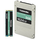
Toshiba Memory Corporation, the world leader in memory solutions, today announced the launch of the SG6 series, a new line-up of SATA client SSDs utilizing Toshiba Memory Corporation's cutting-edge 64-layer, 3-bit-per-cell (TLC) BiCS FLASH. Sample shipments to PC OEM customers start today in limited quantities, and Toshiba Memory Corporation will gradually increase shipments from the fourth calendar quarter of this year.

The new SG6 series SSDs features a SATA Revision 3.3, 6.0Gbit/s interface, and delivers performance of up to 550MB/s sequential read and 535MB/s sequential write. Thanks to improved flash memory management and performance, active power consumption is cut by approximately 40% compared to previous generation products. This improvement can extend battery life, a plus for many applications including mobile computing.

Intel Further Delivers on Storage Transformation with New SSD Form Factor

Today, Intel announces major data center storage advances, reiterating Intel's memory technology leadership. The new technologies advance data center storage and deliver innovative solutions to meet the challenges presented by the growing reliance on data. They include:
  • "Ruler" form factor for Intel SSDs, an all-new solid state drive form factor enabling up to 1PB of storage in a 1U server rack in the future.
  • The world's most advanced dual port portfolio: Intel Optane technology dual port SSDs and Intel 3D NAND dual port SSDs for mission-critical applications.
  • An updated SATA family of SSDs for data center, targeted at HDD replacement.
"We are in the midst of an era of major data center transformation, driven by Intel. These new "ruler" form factor SSDs and dual port SSDs are the latest in a long line of innovations we've brought to market to make storing and accessing data easier and faster, while delivering more value to customers," said Bill Leszinske, Intel vice president, Non-Volatile Memory Solutions Group (NSG), and director, strategic planning, marketing and business development. "Data drives everything we do - from financial decisions to virtual reality gaming, and from autonomous driving to machine learning - and Intel storage innovations like these ensure incredibly quick, reliable access to that data."

Toshiba Introduces World's First Enterprise-Class SSDs with 64-Layer 3D Flash Me

Toshiba America Electronic Components, Inc. (TAEC), a committed technology leader, today unveiled the development of two new flagship enterprise solid state drive (SSD) solutions, the TMC PM5 12 Gbit/s SAS series and the CM5 NVM Express (NVMe) series. Development is expected to be completed in the fourth quarter. Both product lines are built with TMC's latest 64 layer, 3-bit-per-cell enterprise-class TLC (triple-level cell) BiCS FLASH2, making it possible for today's demanding storage environments to expand the use of flash with cost-optimized 3D flash memory. With all-new, advanced features, the innovative CM5 and PM5 series raise the bar in performance capabilities and create new opportunities for businesses to leverage the power of flash storage.

Offering up to 30.72TB in a 2.5-inch form factor, the TMC PM5 series introduces a full range of endurance and capacity SAS SSDs enabling data centers to effectively address big data demands while streamlining storage deployments. With the industry's first MultiLink SAS architecture, the PM5 series is able to deliver the fastest performance the market has seen from a SAS-based SSD with up to 3,350 MB/s of sequential read and 2,720 MB/s of sequential write6 in MultiLink mode and up to 400,000 random read IOPS in narrow or MultiLink mode. The PM5 series' 4-port MultiLink design is an additional technology to achieve high performance, close to PCI EXPRESS (PCIe)8 SSDs, enabling legacy infrastructures to increase productivity without having to be re-architected from the ground up. Furthermore, PM5 SSDs support multi-stream write technology, a feature that intelligently manages and groups data types to minimize write amplification and minimize garbage collection, translating into reduced latency, improved endurance, increased performance and Quality of Service (QoS).

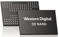
Western Digital Announces Four-Bits-Per-Cell (X4) Technology on 3D NAND

Western Digital Corp. today announced its successful development of four bits per cell, X4, flash memory architecture offering on 64-layer 3D NAND, BiCS3, technology. Building on its pioneering innovation of X4 for 2D NAND technology and past success in commercializing it, the company has now developed X4 for 3D NAND by leveraging its deep vertical integration capabilities. These include silicon wafer processing, device engineering to provide sixteen distinct data levels in every storage node, and system expertise for overall flash management. BiCS3 X4 technology delivers an industry-leading storage capacity of 768 gigabits on a single chip, a 50 percent increase from the prior 512 gigabit chip that was enabled with the three bits per cell (X3) architecture. Western Digital will showcase removable products and solid-state drives built with BiCS3 X4 and systems capabilities in August at the Flash Memory Summit in Santa Clara, California.

"The implementation of X4 architecture on BiCS3 is a significant development for Western Digital as it demonstrates our continued leadership in NAND flash technology, and it also enables us to offer an expanded choice of storage solutions for our customers," said Dr. Siva Sivaram, executive vice president, Memory Technology, Western Digital. "The most striking aspect in today's announcement is the use of innovative techniques in the X4 architecture that allows our BiCS3 X4 to deliver performance attributes comparable to those in BiCS3 X3. The narrowing of the performance gap between the X4 and X3 architectures is an important and differentiating capability for us, and it should help drive broader market acceptance of X4 technology over the next several years."

Toshiba Develops World's First 3D Flash Memory with TSV Technology

Toshiba Memory Corporation, the world leader in memory solutions, today announced development of the world's first BiCS FLASH three-dimensional (3D) flash memory utilizing Through Silicon Via (TSV) technology with 3-bit-per-cell (triple-level cell, TLC) technology. Shipments of prototypes for development purposes started in June, and product samples are scheduled for release in the second half of 2017. The prototype of this groundbreaking device will be showcased at the 2017 Flash Memory Summit in Santa Clara, California, United States, from August 7-10.

Devices fabricated with TSV technology have vertical electrodes and vias that pass through silicon dies to provide connections, an architecture that realizes high speed data input and output while reducing power consumption. Real-world performance has been proven previously, with the introduction of Toshiba's 2D NAND Flash memory.

Toshiba Develops World's First 4-bit Per Cell QLC NAND Flash Memory

Toshiba America Electronic Components, Inc. (TAEC) today announced the latest generation of its BiCS FLASH three-dimensional (3D) flash memory. The newest BiCS FLASH device features 4-bit-per-cell, quadruple-level cell (QLC) technology and is the first 3D flash memory device to do so. Toshiba's QLC technology enables larger (768 gigabit) die capacity than the company's third-generation 512Gb 3-bit-per-cell, triple-level cell (TLC), and pushes the boundaries of flash memory technology.

Toshiba's new QLC BiCS FLASH device features a 64-layer stacked cell structure and achieves the world's largest die capacity (768Gb/96GB). QLC flash memory also enables a 1.5-terabyte (TB) device with a 16-die stacked architecture in a single package - featuring the industry's largest capacity. This is a fifty percent increase in capacity per package when compared to Toshiba's earlier announcement of a 1TB device with a 16-die stacked architecture in a single package - which also offered the largest capacity in the industry at the time.

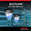
Toshiba Now Shipping Samples of 64-Layer, 512-gigabit 3D Flash Memory

Toshiba Corporation has today unveiled the latest addition in its industry-leading line-up of BiCS FLASH three-dimensional flash memory with a stacked cell structure, a 64-layer device that achieves a 512-gigabit (64-gigabytes) capacity with 3-bit-per-cell (triple-level cell, TLC) technology. The new device will be used in applications that include enterprise and consumer SSD. Sample shipments of the chip started this month, and mass production is scheduled for the second half of this calendar year.

Toshiba continues to refine BiCS FLASH, and the next milestone on its development roadmap is the industry's largest capacity, a 1-terabyte product with a 16-die stacked architecture in a single package. Plans call for the start of sample shipments in April 2017. For the new 512-gigabit device, Toshiba deployed leading-edge 64-layer stacking process to realize a 65% larger capacity per unit chip size than the 48-layer 256-gigabit (32-gigabytes) device, and has increased memory capacity per silicon wafer, reducing the cost per bit.

Seagate Accelerates Enterprise Momentum With Two New Flash Products

Seagate Technology announced today at the Flash Memory Summit conference two new flash innovations that extend the limits of storage computing performance in enterprise data centers to unprecedented levels. The new products include a 60 terabyte (TB) Serial Attached SCSI (SAS) solid-state-drive (SSD) - the largest SSD ever demonstrated - and the 8TB Nytro XP7200 NVMe SSD. These two new products represent the high performance end of Seagate's Enterprise portfolio - a complete ecosystem of HDD, SSD and storage system products designed to help customers manage the deluge of data they face and move the right data where it's needed fast to meet rapidly evolving business priorities and market demands.

The 60TB SAS SSD and 8TB Nytro XP7200 NVMe SSD are the newest additions to Seagate's data center portfolio and are designed to help enterprise IT leaders obtain more value from the rapidly expanding amount of data they must contend with, even under the most demanding application requirements. The 60TB SAS SSD features twice the density and four times the capacity of the next highest-capacity SSD available today - equivalent to the capacity needed to accommodate 400 million photos on a typical social media platform, or 12,000 DVD movies. This single controller architecture also delivers the lowest cost per gigabyte for flash available today.

Samsung Unveils Massive 32 TB SSD Leveraging 64-layer 3D V-NAND

At the 2016 Flash Memory Summit, Samsung unveiled a massive 32-terabyte solid state drive (SSD) for enterprise applications. The drive leverages the company's 4th generation, 64-layer 3D V-NAND flash memory, making it the company's highest-capacity SSD, upping the 15.36 TB drive the company unveiled in March, 2016. The drive is built in the 12 mm-thick, 2.5-inch form-factor, and features the SAS 12 Gb/s interface. At the summit, the company announced that it plans to have 100 TB SSDs ready by 2020.

VIA to Unveil its Latest SSD Controllers at FMS 2016

VIA Technologies, Inc, today announced that it be will demonstrating its latest VIA NVMe PCIe Gen III & SATA III SSD controllers in Booth#818 of the 2016 Flash Memory Summit being held from August 9th to 11th in the Santa Clara Convention Center, California, USA. Featuring the VIA LDPC PLUS ECC decoding engine with Gear-Shifting technology, the second generation VIA SSD controllers offer best-in-class error correction capability and ensure high-throughput performance without overheating issues.

"VIA Gear-Shifting technology leverages our unique dual hardware decoding architecture to maximize data integrity and longevity," said Richard Brown, VP International Marketing, VIA Technologies, Inc. "Our second generation VIA SSD controllers are the ideal choice for computing devices that require superior SSD performance with high cost-efficiency."

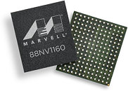
Marvell Introduces the 88NV1160 DRAM-less SSD Controller

Marvell, a world leader in storage, cloud infrastructure, Internet of Things (IoT), connectivity and multimedia semiconductor solutions, today announced the expansion of its solid-state drive (SSD) portfolio to include the 88NV1160 Non-Volatile Memory (NVM) Express DRAM-less SSD controller. Marvell's 88NV1160 DRAM-less SSD controller provides the industry's leading performance per Watt and up to 1600MB/s read speeds. The 88NV1160 can be used in a single ball grid array (BGA) package SSD, as well as in a standalone controller in a tiny 9x10mm package which makes it compatible with M.2230 and M.2242 form factors. These features make the 88NV1160 optimized for a new generation of slim computing devices such as productivity tablets and ultrabooks. The new controller is currently available for sampling to key customers globally.

"As the world's leading storage controller provider, Marvell has a long track record of bringing to market world-class innovations, including the pioneering integration of Host Memory Buffer technology into DRAM-less products. Working closely with other ecosystem leaders, Marvell has continued to advance the industry and drive a new generation of low power, small form factor mobile computing systems," said Dr. David Chen, Vice President of SSD Business at Marvell Semiconductor, Inc. "The 88NV1160 controller is optimally engineered for high performance tablets and ultrabooks, providing unparalleled performance per Watt and the largest NAND compatibility on the market."

SMART Modular Announces Industry's First 32GB DDR4 NVDIMM-N

SMART Modular Technologies, Inc., a leader in specialty memory, storage and hybrid solutions including memory modules, Flash memory cards and other solid state storage products, today announced sample availability of its 32GB DDR4 NVDIMM-N, making it the highest density DDR4 NVDIMM-N module available in the industry. SMART will begin sampling at the end of August 2016. The new 32GB density significantly improves application performance making it ideal in server and storage environments.

NVDIMMs transform main DRAM memory into persistent memory, resulting in higher performing servers by allowing big data, transaction logs, and other latency and performance-sensitive data to be accessed at DRAM speeds without the risk of data loss. Rather than reading and writing data or transaction logs to traditional storage media such as SATA SSDs, PCIe NVMe SSDs, or HDDs, data can be written to and read from main memory without the risk of data loss due to any catastrophic power loss event. Server performance as measured by lower latency, higher IOPS, and greater endurance, all dramatically increase with the integration of NVDIMMs.

Toshiba Announces New BG SSDs with 3-Bit-Per-Cell (TLC) BiCS Flash

Toshiba America Electronic Components, Inc. (TAEC), a committed technology leader, will showcase its new BG series solid state drive (SSD) family featuring cutting-edge BiCS FLASH with 3-bit-per-cell TLC (triple-level cell) technology and Toshiba's new single-package ball grid array (BGA) NVMe PCI Express (PCIe) Gen3 x2 SSD at the 2016 Flash Memory Summit held in Santa Clara, California between August 8 - 11. Delivering a smaller footprint, lower power consumption and better performance than traditional storage options, the BG SSD series is purpose-built for the future wave of ultra-thin mobile PCs, including 2-in-1 convertible notebooks and tablets.

With a surface area 95 percent smaller than conventional 2.5-inch SATA storage devices and 82 percent smaller than M.2 Type 22806, the Toshiba BG series condenses both the controller and NAND flash memory in a single 16 mm x 20 mm BGA package enabling device manufacturers to prioritize features like battery capacity for longer operating times. The BG series is also available mounted on a M.2 Type 22307 module for applications requiring socketed storage. BG SSDs utilize BiCS FLASH, a three-dimensional (3D) stacked cell structure, making it possible to accommodate up to 512 GB of storage capacity in this high-performance and compact form factor. Additionally, the BG series SSDs utilize an in-house Toshiba-developed controller and firmware for a full, vertically developed solution, ensuring technology is tightly integrated for optimal performance, power consumption and reliability.

Samsung Introduces World's Highest Capacity Enterprise SSD - 15.36 TB

Samsung Electronics Co., Ltd., the world leader in advanced memory technology, announced today that it is now shipping the industry's largest solid state drive (SSD) - the "PM1633a," a 15.36 terabyte (TB) drive. First revealed at the 2015 Flash Memory Summit in August, the 15.36TB SSD is based on a 12Gb/s Serial Attached SCSI (SAS) interface, for use in enterprise storage systems. Because the PM1633a comes in a 2.5-inch form factor, enterprise storage managers can fit twice as many of the drives in a standard 19-inch, 2U rack, compared to an equivalent 3.5-inch storage drive

"To satisfy an increasing market need for ultra-high-capacity SAS SSDs from leading enterprise storage system manufacturers, we are directing our best efforts toward meeting our customers' SSD requests," said Jung-bae Lee, Senior Vice President, Memory Product Planning and Application Engineering Team, Samsung Electronics. "We will continue to lead the industry with next-generation SSDs, using our advanced 3D V-NAND memory technology, in order to accelerate the growth of the premium memory market while delivering greater performance and efficiency to our customers."

Toshiba Launches Client SSDs Using 15nm TLC NAND Flash Memory

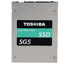
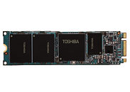
Toshiba Corporation's Semiconductor & Storage Products Company today announced the launch of the "SG5 series" of client SSDs integrating NAND chips fabricated with 15nm TLC process technology. The new products, which include high capacity 1024GB models, will be available in 2.5-type and M.2 2280 (single- and double-sided) form factors, to meet various mounting requirements from the expansion of SSD application fields. Sample shipments start from today.

The SG5 series is equipped with Toshiba's proprietary QSBC (Quadruple Swing-By Code) error correction technology, a highly efficient error correction code (ECC) which helps protect customer data from corruption and improves reliability. Toshiba will continue strengthening its SSD lineup, meeting the various needs of users and leading the continuously expanding SSD market.

Lite-On Unveils EP2 U.2 Enterprise SSDs, and the First Value Data Center SSDs

Lite-On Storage Group, a global leader in the design, development and manufacturing of solid-state drives (SSDs) will be showcasing their latest enterprise and client storage solutions at its Aria suite this year for CES 2016. Lite-On announced its EP2 NVMe M.2 PCIe SSD at the Flash Memory Summit (FMS) 2015. At CES 2016, they are releasing the new addition EP2 PCIe Gen 3 x 4, NVMe 2.5" SSD with U.2 form factor.

The EP2 with the U.2 connector is hot swappable, providing great flexibility to IT Managers to easily change drives without shutting down the server. By combining the PCIe form factor with NVMe protocol, the EP2 U.2 series increase server application performance, lowers latency and delivers fast and predictable data access in a datacenter environment. It delivers superior speed with 4KB random read performance of up to 290,000 IOPS, and 4KB write performance of up to 26,000 IOPS. The EP2 U.2 also features end-to-end data protection, guarding against corruption and errors, and Power Loss Protection, against sudden power loss. The EP2 U.2 is available up to 2TB capacity.

Toshiba Launches New NAND Flash Memory Products for Embedded Applications

Toshiba today launched a new line-up of NAND flash memory products for embedded applications that are compatible with the widely used Serial Peripheral Interface (SPI). Wide ranging applications for the new "Serial Interface NAND" include such consumer applications as flat-screen TVs, printers and wearable devices, and industrial applications, including robots. Users can choose from a wide line-up of 12 products that offers three densities, 1Gbit, 2Gbit and 4Gbit; two packages, WSON[1] and SOP[2] and two power supply voltages. Samples shipment starts today and mass production is scheduled to begin with the 1Gbit products from December. Mass production of the remaining line-up will follow.

Compatibility with the widely used SPI, which can be controlled with just six pins, allows the new "Serial Interface NAND" to be used as SLC NAND flash memory, with a low pin count, small package and large capacity.

Samsung Shows Off its Biggest and Fastest SSDs at FMS 2015

At the 2015 Flash Memory Summit, Samsung announced the fruition of its swanky new 48-layer 3D V-NAND chips, the PM1633a. Built in the 2.5-inch form-factor, and featuring a SAS 12 Gb/s interface, this drive offers an unformatted capacity nearing 16 TB (15,360 GB to be precise). The drive relies on ten 48-layer stacks of 256 Gb 3-bit NAND flash dies, making up 15,360 GB of unformatted capacity. Samsung showed off a system with 48 of these drives, making up 720 TB of total storage.

Besides the largest SSD, Samsung also showed off the fastest. The PM1725 SSD, designed for servers with high-traffic databases, where throughput is the king, is built in the 2.5-inch form factor (up to 3.2 TB) and HHHL form-factor (up to 6.4 TB). It features a PCI-Express 3.0 host bus, and talks to the OS over the modern NVMe protocol. The two offer random access throughput of up to 1,000,000 IOPS.

Toshiba Develops First 16-die Stacked NAND Flash Memory with TSV Technology

Toshiba Corporation today announced the development of the world's first 16-die (max.) stacked NAND flash memory utilizing Through Silicon Via (TSV) technology. The prototype will be shown at Flash Memory Summit 2015, to be held from August 11 to 13 in Santa Clara, USA.

The prior art of stacked NAND flash memories are connected together with wire bonding in a package. TSV technology instead utilizes the vertical electrodes and vias to pass through the silicon dies for the connection. This enables high speed data input and output, and reduces power consumption.

Transcend Launches New e.MMC Memory Chips

Transcend Information, Inc. (Transcend), a leading manufacturer of industrial-grade products, is proud to announce the launch of the new EMC210 e.MMC (embedded Multi-Media Card) storage solution. The MLC-based EMC210 features simplified interface design, enhanced storage capacities, upgraded performance and a set of comprehensive functions. The small factor e.MMC is an embedded storage ideal for mobile devices, embedded devices and industrial applications, and is compliant with JEDEC (Joint Electron Device Engineering Council) version 4.51 standards.

The e.MMC is comprised of the NAND Flash and the Flash Memory Controller in a 153-ball BGA package. By integrating the controller into the flash memory package, the e.MMC supports the MMC interface and streamlines the development of new products that comply with a simpler set of industry-standard specifications for memory management. Transcend's e.MMC solution provides greater flexibility with interface voltage of either 1.65~1.95V or 2.7V~3.6V. Consequently, manufacturers can benefit from a more efficient design process, lower costs, and reduced time-to-market for end products.

Micron and Intel Unveil New 3D NAND Flash Memory

Micron Technology, Inc., and Intel Corporation today revealed the availability of their 3D NAND technology, the world's highest-density flash memory. Flash is the storage technology used inside the lightest laptops, fastest data centers, and nearly every cellphone, tablet and mobile device.

This new 3D NAND technology, which was jointly developed by Intel and Micron, stacks layers of data storage cells vertically with extraordinary precision to create storage devices with three times higher capacity than competing NAND technologies. This enables more storage in a smaller space, bringing significant cost savings, low power usage and high performance to a range of mobile consumer devices as well as the most demanding enterprise deployments.

Samsung Introduces 128GB 3-bit NAND Flash Memory Storage Device

Samsung Electronics Co., Ltd., the world leader in advanced memory technology, today introduced a high-performance mobile memory storage based on Embedded MultiMediaCard (eMMC) 5.0 technology. The new 128-gigabyte (GB), 3-bit NAND-based eMMC 5.0 storage is targeted at the smartphone and tablet mass markets.

"With the introduction of our value-focused, 3-bit NAND-based eMMC 5.0 line-up, we expect to take the lead in the expansion of high-density mobile storage," said Dr. Jung-Bae Lee, Senior Vice President of Memory Product Planning and Application Engineering Team, Samsung Electronics. "We are continuing to enhance our next-generation embedded mobile memory offerings with improved performance and higher densities to meet increasing customer demand across the mobile industry."

Samsung Starts Mass Production of Industry's First 3-bit 3D V-NAND Flash Memory

Samsung Electronics Co., Ltd., the world leader in advanced memory technology, today announced that it has begun mass producing the industry's first 3-bit multi-level-cell (MLC) three-dimensional (3D) Vertical NAND (V-NAND) flash memory, for use in solid state drives (SSDs).

"With the addition of a whole new line of high density SSDs that is both performance- and value-driven, we believe the 3-bit V-NAND will accelerate the transition of data storage devices from hard disk drives to SSDs," said Jaesoo Han, Senior Vice President, Memory Sales & Marketing, Samsung Electronics. "The wider variety of SSDs will increase our product competitiveness as we further expand our rapidly growing SSD business."

The 3-bit V-NAND is Samsung's latest second generation V-NAND device, which utilizes 32 vertically stacked cell layers per NAND memory chip. Each chip provides 128 gigabits (Gb) of memory storage.

Toshiba Offers World's Smallest-Class e-MMC Embedded NAND Flash Memory Products

Toshiba America Electronic Components, Inc., (TAEC), a committed leader that collaborates with technology companies to create breakthrough designs, today announced the launch of a class of e-MMCTM embedded NAND flash memory products that are among the world's smallest.The new products integrate NAND chips fabricated with Toshiba's cutting-edge 15 nm process technology and a controller to manage basic control functions for NAND applications into a single package.

Fully compliant with the latest JEDEC e-MMC standard, the new chips are designed for application in a wide range of digital consumer products, including smartphones, tablet PCs and wearable devices. Sample shipment of the 16 gigabyte (GB) products begins today, with 8GB, 32GB, 64GB, and 128GB products to follow. By utilizing the 15nm process technology, the new product's package size is approximately 26 percent smaller than comparable Toshiba products and offers faster read/write performance due to improvements in basic chip performance and controller optimization. The read speed is approximately eight percent faster (max.), while the write speed is approximately 20 percent faster (max.).

Toshiba Introduces EXCERIA UHS-I SD Memory Cards

Toshiba's Digital Products Division (DPD), a division of Toshiba America Information Systems, Inc., today introduced EXCERIA UHS-I SD Memory Cards, a new line of EXCERIA products focused on continuous shooting and full HD (including 4K resolution) video, a perfect fit for professional or amateur photographers in a wide-range of sizes at an affordable price.

Great for professional DSLR photographers, videographers and content creators who demand high-performance tools, these EXCERIA SD cards offer faster write speeds than Class 10 SD cards, have greater mobile storage capacity (up to 128GB) than other EXCERIA products and include UHS Speed Class 3 (U3) support for 4K2K video recording and playback. With EXCERIA UHS-I SD cards, digital pros, enthusiast photographers and amateurs can enjoy fast-motion capture and playback of high-resolution content, plus the benefits of high-speed continuous shooting, real-time full HD video recording and the time-saving value of lightning-fast data transfers for large files. With EXCERIA, backing up 1,000 photographs takes only one-third the time needed by other UHS-I SD cards.
Return to Keyword Browsing
Nov 21st, 2024 12:11 EST change timezone

New Forum Posts

Popular Reviews

Controversial News Posts