News Posts matching #HPC

Return to Keyword Browsing

Samsung Expands its Foundry Capacity with A New Production Line in Pyeongtaek

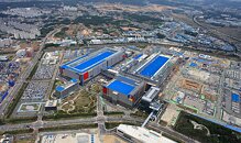
Samsung Electronics Co., Ltd., a world leader in advanced semiconductor technology, today announced plans to boost its foundry capacity at the company's new production line in Pyeongtaek, Korea, to meet growing global demand for cutting-edge extreme ultraviolet (EUV) solutions.

The new foundry line, which will focus on EUV-based 5 nanometer (nm) and below process technology, has just commenced construction this month and is expected to be in full operation in the second half of 2021. It will play a pivotal role as Samsung aims to expand the use of state-of-the-art process technologies across a myriad of current and next generation applications, including 5G, high-performance computing (HPC) and artificial intelligence (AI).
Atos Launches First Supercomputer Equipped with NVIDIA A100 Tensor Core GPU

Atos, a global leader in digital transformation, today announces its new BullSequana X2415, the first supercomputer in Europe to integrate NVIDIA's Ampere next-generation graphics processing unit architecture, the NVIDIA A100 Tensor Core GPU. This new supercomputer blade will deliver unprecedented computing power to boost application performance for HPC and AI workloads, tackling the challenges of the exascale era. The BullSequana X2415 blade will increase computing power by more than 2x and optimize energy consumption thanks to Atos' 100% highly efficient water-cooled patented DLC (Direct Liquid Cooling) solution, which uses warm water to cool the machine.

Forschungszentrum Jülich will integrate this new blade into its booster module, extending its existing JUWELS BullSequana supercomputer, making it the first system worldwide the use this new technology. The JUWELS Booster will provide researchers across Europe with significantly increased computational resources. Some of the projects it will fuel are the European Commission's Human Brain Project and the Jülich Laboratories of "Climate Science" and "Molecular Systems". Once fully deployed this summer the upgraded supercomputing system, operated under ParTec's software ParaStation Modulo, is expected to provide a computational peak performance of more than 70 Petaflops/s making it the most powerful supercomputer in Europe and a showcase for European exascale architecture.

NVIDIA Announces Industry's First Secure SmartNIC Optimized for 25G

NVIDIA today launched the NVIDIA Mellanox ConnectX -6 Lx SmartNIC—a highly secure and efficient 25/50 gigabit per second (Gb/s) Ethernet smart network interface controller (SmartNIC)—to meet surging growth in enterprise and cloud scale-out workloads.

ConnectX-6 Lx, the 11th generation product in the ConnectX family, is designed to meet the needs of modern data centers, where 25 Gb/s connections are becoming standard for handling demanding workflows, such as enterprise applications, AI and real-time analytics. The new SmartNIC extends accelerated computing by leveraging software-defined, hardware-accelerated engines to offload more security and network processing from CPUs.
NVIDIA Mellanox ConnectX-6 Lx SmartNIC

AMD Announces Radeon Pro VII Graphics Card, Brings Back Multi-GPU Bridge

AMD today announced its Radeon Pro VII professional graphics card targeting 3D artists, engineering professionals, broadcast media professionals, and HPC researchers. The card is based on AMD's "Vega 20" multi-chip module that incorporates a 7 nm (TSMC N7) GPU die, along with a 4096-bit wide HBM2 memory interface, and four memory stacks adding up to 16 GB of video memory. The GPU die is configured with 3,840 stream processors across 60 compute units, 240 TMUs, and 64 ROPs. The card is built in a workstation-optimized add-on card form-factor (rear-facing power connectors and lateral-blower cooling solution).

What separates the Radeon Pro VII from last year's Radeon VII is full double precision floating point support, which is 1:2 FP32 throughput compared to the Radeon VII, which is locked to 1:4 FP32. Specifically, the Radeon Pro VII offers 6.55 TFLOPs double-precision floating point performance (vs. 3.36 TFLOPs on the Radeon VII). Another major difference is the physical Infinity Fabric bridge interface, which lets you pair up to two of these cards in a multi-GPU setup to double the memory capacity, to 32 GB. Each GPU has two Infinity Fabric links, running at 1333 MHz, with a per-direction bandwidth of 42 GB/s. This brings the total bidirectional bandwidth to a whopping 168 GB/s—more than twice the PCIe 4.0 x16 limit of 64 GB/s.

Graphics Cards Shipments to Pick Up in 2H-2020: Cooling Solution Maker Power Logic

Power Logic, a graphics card cooling solution OEM, in an interview with Taiwan tech industry observer DigiTimes, commented that it expects graphics card shipments to rise in the second half of 2020, on the backs of new product announcements from both NVIDIA and AMD, as well as HPC accelerators from the likes of Intel and NVIDIA. NVIDIA is expected to launch its "Ampere" based GeForce RTX 30-series graphics cards, while AMD is preparing to launch its Radeon RX 6000-series "Navi 2#" graphics cards based on the RDNA2 graphics architecture. Power Logic has apparently commenced prototyping certain cooling solutions, and is expected to begin mass-production at its Jiangxi-based plant towards the end of Q2-2020; so it could begin shipping coolers to graphics card manufacturers in the following quarters.

TSMC Secures Orders from NVIDIA for 7nm and 5nm Chips

TSMC has reportedly secured orders from NVIDIA for chips based on its 7 nm and 5 nm silicon fabrication nodes, sources tell DigiTimes. If true, it could confirm rumors of NVIDIA splitting its next-generation GPU manufacturing between TSMC and Samsung. The Korean semiconductor giant is commencing 5 nm EUV mass production within Q2-2020, and NVIDIA is expected to be one of its customers. NVIDIA is expected to shed light on its next-gen graphics architecture at the GTC 2020 online event held later this month. With its "Turing" architecture approaching six quarters of market presence, it's likely that the decks are being cleared for a new architecture not just in HPC/AI compute product segment, but also GeForce and Quadro consumer graphics cards. Splitting manufacturing between TSMC and Samsung would help NVIDIA disperse any yield issue arriving from either foundry's EUV node, and give it greater bargaining power with both.

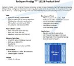
Tachyum Prodigy is a Small 128-core Processor with Crazy I/O Options, 64-core Sibling Enroute Production

Silicon Valley startup Tachyum, founded in 2016, is ready with its crowning product, the Tachyum Prodigy. The startup recently received an investment from the Slovak government in hopes of job-creation in the country. The Prodigy is what its makers call "a universal processor," which "outperforms the fastest Xeon at 10X lower power." The company won't mention what machine architecture it uses (whether it's Arm or MIPS, or its own architecture). Its data-sheet is otherwise full of specs that scream at you.

To begin with, its top trim, the Prodigy T16128, packs 128 cores on a single package, complete with 64-bit address space, 512-bit vector extensions, matrix multiplication fixed-function hardware that accelerate AI/ML, and 4 IPC at up to 4.00 GHz core clock. Tachyum began the processor's software-side support, with an FPGA emulator in December 2019 (so you can emulate the processor on an FPGA and begin developing for it), C/C++ and Fortran compilers; debuggers and profilers, tensorflow compilers, and a Linux distribution that's optimized it. The I/O capabilities of this chip are something else.

NERSC Finalizes Contract for Perlmutter Supercomputer Powered by AMD Milan and NVIDIA Volta-Successor

The National Energy Research Scientific Computing Center (NERSC), the mission high-performance computing facility for the U.S. Department of Energy's Office of Science, has moved another step closer to making Perlmutter - its next-generation GPU-accelerated supercomputer - available to the science community in 2020.

In mid-April, NERSC finalized its contract with Cray - which was acquired by Hewlett Packard Enterprise (HPE) in September 2019 - for the new system, a Cray Shasta supercomputer that will feature 24 cabinets and provide 3-4 times the capability of NERSC's current supercomputer, Cori. Perlmutter will be deployed at NERSC in two phases: the first set of 12 cabinets, featuring GPU-accelerated nodes, will arrive in late 2020; the second set, featuring CPU-only nodes, will arrive in mid-2021. A 35-petabyte all-flash Lustre-based file system using HPE's ClusterStor E1000 hardware will also be deployed in late 2020.

NVIDIA Acquires Network-Software Trailblazer Cumulus

Cloud data centers are evolving to an architecture that is accelerated, disaggregated and software-defined to meet the exponential growth in AI and high performance computing. To build these modern data centers, HPC and networking hardware and software must go hand in hand. NVIDIA provides the leading accelerated computing platform. Mellanox is the high-performance networking leader, now part of NVIDIA in a combination described in our founder and CEO's welcome letter.

Today we announce our plan to acquire Cumulus Networks, bolstering our networking software capabilities. The combination enables the new era of the accelerated, software-defined data center. With Cumulus, NVIDIA can innovate and optimize across the entire networking stack from chips and systems to software including analytics like Cumulus NetQ, delivering great performance and value to customers. This open networking platform is extensible and allows enterprise and cloud-scale data centers full control over their operations.

NVIDIA DGX A100 is its "Ampere" Based Deep-learning Powerhouse

NVIDIA will give its DGX line of pre-built deep-learning research workstations its next major update in the form of the DGX A100. This system will likely pack number of the company's upcoming Tesla A100 scalar compute accelerators based on its next-generation "Ampere" architecture and "GA100" silicon. The A100 came to light though fresh trademark applications by the company. As for specs and numbers, we don't know yet. The "Volta" based DGX-2 has up to sixteen "GV100" based Tesla boards adding up to 81,920 CUDA cores and 512 GB of HBM2 memory. One can expect NVIDIA to beat this count. The leading "Ampere" part could be HPC-focused, featuring a large CUDA-, and tensor core count, besides exotic memory such as HBM2E. We should learn more about it at the upcoming GTC 2020 online event.

Intel Teases "Big Daddy" Xe-HP GPU

The Intel Graphics Twitter account was on fire today, because they posted an update on the development of the Xe graphics processor, mentioning that samples are ready and packed up in quite an interesting package. The processor in question was discovered to be a Xe-HP GPU variant with an estimated die size of 3700 mm², which means we sure are talking about a multi-chip package here. How we concluded that it is the Xe-HP GPU, is by words of Raja Koduri, senior vice president, chief architect, general manager for Architecture, Graphics, and Software at Intel. He made a tweet, which was later deleted, that says this processor is a "baap of all", meaning "big daddy of them all" when translated from Hindi.

Mr. Koduri previously tweeted a photo of the Intel Graphics team at India, which has been working on the same "baap of all" GPU, which suggests this is a Xe-HP chip. It seems that this is not the version of the GPU made for HPC workloads (this is reserved for the Xe-HPC GPU), this model could be a direct competitor to offers like NVIDIA Quadro or AMD Radeon Pro. We can't wait to learn more about Intel's Xe GPUs, so stay tuned. Mr. Koduri has confirmed that this GPU will be used only for Data Centric applications as it is needed to "keep up with the data we are generating". He has also added that the focus for gaming GPUs is to start off with better integrated GPUs and low power chips above that, that could reach millions of users. That will be a good beginning as that will enable software preparation for possible high-performance GPUs in future.

Update May 2: changed "father" to "big daddy", as that's the better translation for "baap".
Update 2, May 3rd: The GPU is confirmed to be a Data Center component.

Khronos Group Releases OpenCL 3.0

Today, The Khronos Group, an open consortium of industry-leading companies creating advanced interoperability standards, publicly releases the OpenCL 3.0 Provisional Specifications. OpenCL 3.0 realigns the OpenCL roadmap to enable developer-requested functionality to be broadly deployed by hardware vendors, and it significantly increases deployment flexibility by empowering conformant OpenCL implementations to focus on functionality relevant to their target markets. OpenCL 3.0 also integrates subgroup functionality into the core specification, ships with a new OpenCL C 3.0 language specification, uses a new unified specification format, and introduces extensions for asynchronous data copies to enable a new class of embedded processors. The provisional OpenCL 3.0 specifications enable the developer community to provide feedback on GitHub before the specifications and conformance tests are finalized.
OpenCL

SiPearl Signs Agreement with Arm for the Development of its First-Generation of Microprocessors

SiPearl, the company that is designing the high-performance, low-power microprocessor for the European exascale supercomputer, has signed a major technological licensing agreement with Arm, the global semiconductor IP provider. The agreement will enable SiPearl to benefit from the high-performance, secure, and scalable next-generation Arm Neoverse platform, codenamed ''Zeusʺ, as well as leverage the robust software and hardware Arm ecosystem.

Taking advantage of the Arm "Zeus" platform, including Arm's POP IP, on advanced FinFET technologyenables SiPearl to accelerate its design and ensure outstanding reliability for a very high-end offering,in terms of both computing power and energy efficiency, and be ready to launch its first generation of microprocessors in 2022.
European Procesor Initiative

AMD Donates $15 Million Worth EPYC CPUs and Radeon Instinct Accelerators to aid COVID-19 Research

AMD on April 15 updated its COVID-19 response strategy to include a sizable donation of enterprise hardware from its inventory towards COVID-19 vaccine research. The company is giving away $15 million worth HPCs cloud computing nodes powered by EPYC enterprise processors and Radeon Instinct scalar compute accelerators to key research institutions at the forefront of vaccine research for COVID-19. AMD says that these systems will be of a turnkey nature, so they could be quickly deployed and put to use. The company invites any institution conducting COVID-19 related research to contact them for access to the node.

Making the announcement, CEO Dr. Lisa Su writes: "AMD is announcing today a COVID-19 HPC fund to provide research institutions with computing resources to accelerate medical research on COVID-19 and other diseases. The fund will include an initial donation of $15 million of high-performance systems powered by AMD EPYC CPUs and AMD Radeon Instinct GPUs to key research institutions. To ease the implementation and speed the useful impact from these donations, we are working with our HPC system provider partners to provide ready-to-install HPC nodes. Research institutions should contact AMD at COVID-19HPC[at]amd[dot]com to submit proposals for access to these nodes."

AMD & NVIDIA Join the HPC COVID-19 Consortium

AMD and NVIDIA are the latest computing giants to join the HPC COVID-19 Consortium, they join the likes of Google, Amazon, Microsoft along with the US Federal Government and Academic Institutions in support of COVID-19 research. This announcement brings the combined power of the cluster to 402 petaflops which trails behind the community driven Folding@Home project which holds the record at 1,500 petaflops but is still more powerful than any one supercomputer.

Researchers can apply to the HPC COVID-19 Consortium for compute resources in the fight against COVID-19.
cluster

Micron to Launch HBM2 Memory This Year

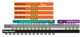
Micron Technologies, in the latest earnings report, announced that they will start shipping High-Bandwidth Memory 2 (HBM2) DRAM. Used for high-performance graphics cards, server processors and all kinds of processors, HBM2 memory is wanted and relatively expensive solution, however, when Micron enters the market of its manufacturing, prices, and the market should adjust for the new player. Previously, only SK-Hynix and Samsung were manufacturing the HBM2 DRAM, however, Micron will join them and they will again form a "big-three" pact that dominates the memory market.

Up until now, Micron used to lay all hopes on its proprietary Hybrid Memory Cube (HMC) DRAM type, which didn't gain much traction from customers and it never really took off. Only a few rare products used it, as Fujitsu SPARC64 XIfx CPU used in Fujitsu PRIMEHPC FX100 supercomputer introduced in 2015. Micron announced to suspend works on HMC in 2018 and decided to devote their efforts to GDDR6 and HBM development. So, as a result, we are seeing that they will launch HBM2 DRAM products sometime this year.
Micron HMC High-Bandwidth Memory

Intel Scales Neuromorphic Research System to 100 Million Neurons

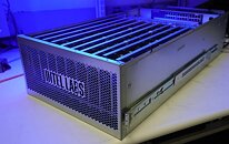
Today, Intel announced the readiness of Pohoiki Springs, its latest and most powerful neuromorphic research system providing the computational capacity of 100 million neurons. The cloud-based system will be made available to members of the Intel Neuromorphic Research Community (INRC), extending their neuromorphic work to solve larger, more complex problems.

"Pohoiki Springs scales up our Loihi neuromorphic research chip by more than 750 times, while operating at a power level of under 500 watts. The system enables our research partners to explore ways to accelerate workloads that run slowly today on conventional architectures, including high-performance computing (HPC) systems." -Mike Davies, director of Intel's Neuromorphic Computing Lab.
Intel Pohoiki Springs Intel Pohoiki Springs Intel Pohoiki Springs Intel Pohoiki Springs

AMD Announces the CDNA and CDNA2 Compute GPU Architectures

AMD at its 2020 Financial Analyst Day event unveiled its upcoming CDNA GPU-based compute accelerator architecture. CDNA will complement the company's graphics-oriented RDNA architecture. While RDNA powers the company's Radeon Pro and Radeon RX client- and enterprise graphics products, CDNA will power compute accelerators such as Radeon Instinct, etc. AMD is having to fork its graphics IP to RDNA and CDNA due to what it described as market-based product differentiation.

Data centers and HPCs using Radeon Instinct accelerators have no use for the GPU's actual graphics rendering capabilities. And so, at a silicon level, AMD is removing the raster graphics hardware, the display and multimedia engines, and other associated components that otherwise take up significant amounts of die area. In their place, AMD is adding fixed-function tensor compute hardware, similar to the tensor cores on certain NVIDIA GPUs.
AMD Datacenter GPU Roadmap CDNA CDNA2 AMD CDNA Architecture AMD Exascale Supercomputer

AMD Financial Analyst Day 2020 Live Blog

AMD Financial Analyst Day presents an opportunity for AMD to talk straight with the finance industry about the company's current financial health, and a taste of what's to come. Guidance and product teasers made during this time are usually very accurate due to the nature of the audience. In this live blog, we will post information from the Financial Analyst Day 2020 as it unfolds.
20:59 UTC: The event has started as of 1 PM PST. CEO Dr Lisa Su takes stage.

Kingston Releases DC1000M U.2 NVMe SSDs for Mixed-use in Data Centers

Kingston Digital, Inc., the Flash memory affiliate of Kingston Technology Company, Inc., a world leader in memory products and technology solutions, today announced the availability of DC1000M, a new U.2 data center NVMe PCIe SSD. DC1000M is designed to support a wide range of data-intensive enterprise workloads, including Cloud computing, web hosting, high-performance computing (HPC), virtual infrastructures, artificial intelligence and deep learning applications. DC1000M joins the recently released DC1000B NVMe boot drive, the VMware Ready DC500 series SATA SSDs and DC450R to form the most complete range of superior enterprise-class data center storage solutions in the market.

"Mission critical services and Cloud-based applications depend not only on lightning-fast IOPS and bandwidth, but also on the consistency and predictability of the data being serviced," said Keith Schimmenti, enterprise SSD business manager, Kingston. "DC1000M provides the stability and low latency for the evolving data center, while powering the workloads that require one drive write per day (1 DWPD) endurance."

Ampere Computing Uncovers 80 Core "Cloud-Native" Arm Processor

Ampere Computing, a startup focusing on making HPC and processors from cloud applications based on Arm Instruction Set Architecture, today announced the release of a first 80 core "cloud-native" processor based on the Arm ISA. The new Ampere Altra CPU is the company's first 80 core CPU meant for hyper scalers like Amazon AWS, Microsoft Azure, and Google Cloud. Being built on TSMC's 7 nm semiconductor manufacturing process, the Altra is a CPU that is utilizing a monolithic die to achieve maximum performance. Using Arm's v8.2+ instruction set, the CPU is using the Neoverse N1 platform as its core, to be ready for any data center workload needed. It also borrows a few security features from v8.3 and v8.5, namely the hardware mitigations of speculative attacks.

When it comes to the core itself, the CPU is running at 3.0 GHz frequency and has some very interesting specifications. The design of the core is such that it is 4-wide superscalar Out of Order Execution (OoOE), which Ampere refers to as "aggressive" meaning that there is a lot of data throughput going on. The cache levels are structured in a way that there is 64 KB of L1D and L1I cache per core, along with 1 MB of L2 cache per core as well. For system-level cache, there is 32 MB of L3 available to the SoC. All of the caches have Error-correcting code (ECC) built-in, giving the CPU a much-needed feature. There are two 128-bit wide Single Instruction Multiple Data (SIMD) units, which are there to do parallel processing if needed. There is no mention if they implement Arm's Scalable Vector Extensions (SVE) or not.

TSMC to Hire 4000 new Staff for Next-Generation Semiconductor Node Development

TSMC is set to hire about 4000 new staff members to gain a workforce for its development of next-generation semiconductor manufacturing nodes. The goal of the company is to gather talent so it can develop the world's leading semiconductor nodes, like 3 nm and below. With 15 billion USD planned for R&D purposes alone this year, TSMC is investing a big part of its capital back into development on new and improved technology. Markets such as 5G and High-Performance Computing are leading the charge and require smaller, faster, and more efficient semiconductor nodes, which TSMC plans to deliver. To gather talent, TSMC started job listing using recruitment website TaiwanJobs and started campaigns on university campuses to attract grad students.

ASUS Announces Exclusive Power Balancer Technology and Servers with New 2nd Gen Intel Xeon Scalable

ASUS, the leading IT Company in server systems, server motherboards, workstations and workstation motherboards today announced exclusive Power Balancer technology to support the new 2nd Gen Intel Xeon Scalable Processor (extended Cascade Lake-SP refresh SKUs) across all server product lineups, including the RS720/720Q/700 E9, RS520/500 E9 and ESC8000/4000 G4 series server systems and Z11 server motherboards.

In complex applications, such as high-performance computing (HPC), AI or edge computing, balancing performance and power consumption is always a challenge. With Power Balancer technology and the new 2nd Gen Intel Xeon Scalable Processor, ASUS servers save up to 31 watts power per node on specific workloads and achieve even better efficiency with more servers in large-scale environments, significantly decreasing overall power consumption for a much lower total cost of ownership and optimized operations.

Samsung Launches 3rd-Generation "Flashbolt" HBM2E Memory

Samsung Electronics, the world leader in advanced memory technology, today announced the market launch of 'Flashbolt', its third-generation High Bandwidth Memory 2E (HBM2E). The new 16-gigabyte (GB) HBM2E is uniquely suited to maximize high performance computing (HPC) systems and help system manufacturers to advance their supercomputers, AI-driven data analytics and state-of-the-art graphics systems in a timely manner.

"With the introduction of the highest performing DRAM available today, we are taking a critical step to enhance our role as the leading innovator in the fast-growing premium memory market," said Cheol Choi, executive vice president of Memory Sales & Marketing at Samsung Electronics. "Samsung will continue to deliver on its commitment to bring truly differentiated solutions as we reinforce our edge in the global memory marketplace."

Europe Readies its First Prototype of Custom HPC Processor

European Processor Initiative (EPI) is a Europe's project to kickstart a homegrown development of custom processors tailored towards different usage models that the European Union might need. The first task of EPI is to create a custom processor for high-performance computing applications like machine learning, and the chip prototypes are already on their way. The EPI chairman of the board Jean-Marc Denis recently spoke to the Next Platform and confirmed some information regarding the processor design goals and the timeframe of launch.

Supposed to be manufactured on TSMC's 6 nm EUV (TSMC N6 EUV) technology, the EPI processor will tape-out at the end of 2020 or the beginning of 2021, and it is going to be heterogeneous. That means that on its 2.5D die, many different IPs will be present. The processor will use a custom ARM CPU, based on a "Zeus" iteration of Neoverese server core, meant for general-purpose computation tasks like running the OS. When it comes to the special-purpose chips, EPI will incorporate a chip named Titan - a RISC-V based processor that uses vector and tensor processing units to compute AI tasks. The Titan will use every new standard for AI processing, including FP32, FP64, INT8, and bfloat16. The system will use HBM memory allocated to the Titan processor, have DDR5 links for the CPU, and feature PCIe 5.0 for the inner connection.
Return to Keyword Browsing
Dec 19th, 2024 00:02 EST change timezone

New Forum Posts

Popular Reviews

Controversial News Posts