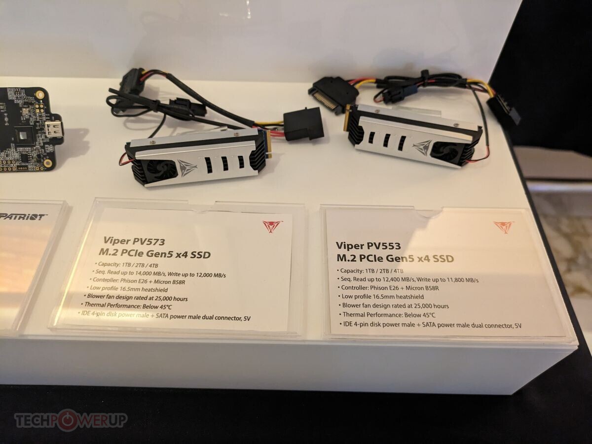
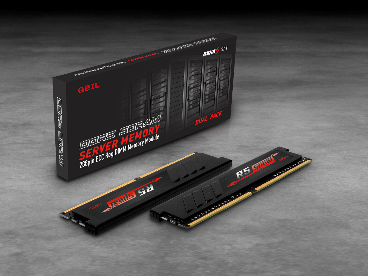
SK Hynix Throws a Jab: CAMM is Coming to Desktop PCs
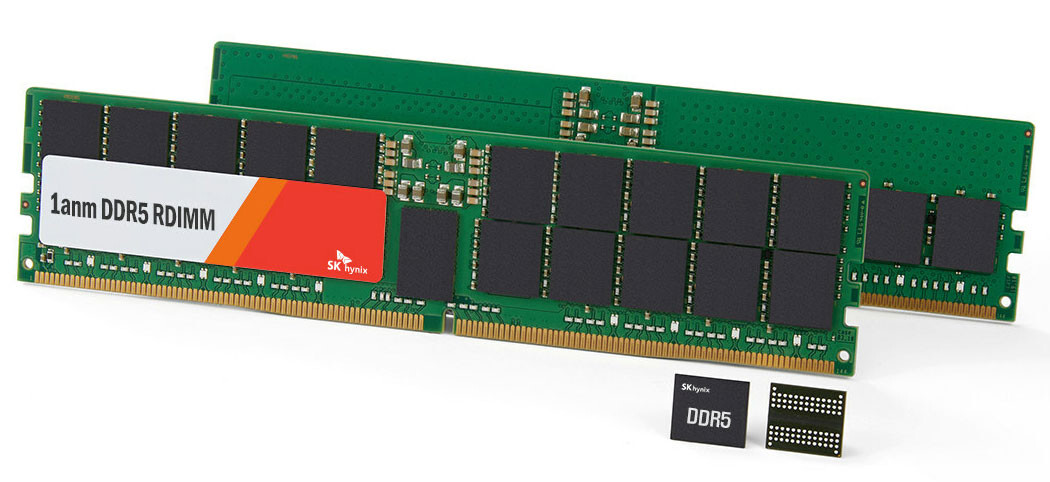
In a surprising turn of events, SK Hynix has hinted at the possibility of the Compression Attached Memory Module (CAMM) standard, initially designed for laptops, being introduced to desktop PCs. This revelation came from a comment made by an SK Hynix representative at the CES 2024 in Las Vegas for the Korean tech media ITSubIssub. According to the SK Hynix representative, the first implementation is underway, but there are no specific details. CAMM, an innovative memory standard developed by Dell in 2022, was certified to replace SO-DIMM as the official standard for laptop memory. However, the transition to desktop PCs could significantly disrupt the desktop memory market. The CAMM modules, unlike the vertical DRAM sticks currently in use, are horizontal and are screwed into a socket. This design change would necessitate a complete overhaul of the desktop motherboard layout.
The thin, flat design of the CAMM modules could also limit the number that can be installed on an ATX board. However, the desktop version of the standard CAMM2 was announced by JEDEC just a month ago. It is designed for DDR5 memory, but it is expected to become mainstream with the introduction of DDR6 around 2025. While CAMM allows for higher speeds and densities for mobile memory, its advantages for desktops over traditional memory sticks are yet to be fully understood. Although low-power CAMM modules could offer energy savings, this is typically more relevant for mobile devices than desktops. As we move towards DDR6 and DDR7, more information about CAMM for desktops will be needed to understand its potential benefits. JEDEC's official words on the new standard indicate that "DDR5 CAMM2s are intended for performance notebooks and mainstream desktops, while LPDDR5/5X CAMM2s target a broader range of notebooks and certain server market segments." So, we can expect to see CAMM2 in both desktops and some server applications.
The thin, flat design of the CAMM modules could also limit the number that can be installed on an ATX board. However, the desktop version of the standard CAMM2 was announced by JEDEC just a month ago. It is designed for DDR5 memory, but it is expected to become mainstream with the introduction of DDR6 around 2025. While CAMM allows for higher speeds and densities for mobile memory, its advantages for desktops over traditional memory sticks are yet to be fully understood. Although low-power CAMM modules could offer energy savings, this is typically more relevant for mobile devices than desktops. As we move towards DDR6 and DDR7, more information about CAMM for desktops will be needed to understand its potential benefits. JEDEC's official words on the new standard indicate that "DDR5 CAMM2s are intended for performance notebooks and mainstream desktops, while LPDDR5/5X CAMM2s target a broader range of notebooks and certain server market segments." So, we can expect to see CAMM2 in both desktops and some server applications.