News Posts matching #JEDEC

Return to Keyword Browsing

SK Hynix Announces 1Ynm 16Gb DDR5 DRAM

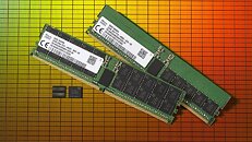
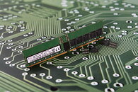
SK Hynix announced that it has developed 16 Gb DDR5 DRAM, the industry's first DDR5 to meet the JEDEC standards. The same 1Ynm process technology used for the recently-developed 1Ynm 8Gb DDR4 DRAM was applied to the new DRAM, giving an industry-leading competitive edge for the Company.

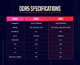
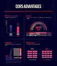
DDR5 is a next-generation DRAM standard that offers ultra-high speed and high density with reduced power consumption as compared to DDR4, for use in data-intensive applications such as big data, artificial intelligence, and machine learning.

Crucial Expands Server Memory Portfolio with First 32GB NVDIMM Offering

Crucial , a leading global consumer brand of Micron Technology for memory and storage upgrades, today announced a new 32GB Nonvolatile DIMM (NVDIMM) to help companies preserve critical data in the event of a system power loss and limit costly downtime. The first Crucial NVDIMM to operate at 2933 MT/s, the new module provides companies powerful and persistent memory performance while reducing the amount of NVDIMMs needed in a server.

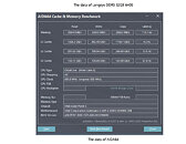
In fast-paced business environments, sales and customer satisfaction are decided in milliseconds. Crucial NVDIMMs give organisations the advantage when data transactions hang in the balance by fusing memory with on-module NAND, providing near-instant access with data persistence. In the event of a system power loss, the NVDIMM would back up DRAM data to the NAND with help from an ultracapacitator, its backup power source. Crucial NVDIMMs are compatible with the latest 2.5 inch drive bay and HHHL PCIe AgigA Tech PowerGEM ultracapacitors, enabling continual power to up to four NVDIMMs during power loss until a backup is completed.

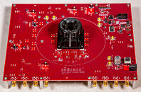
Cadence, Micron Update on DDR5: Still On Track, 1.36x Performance Increase Over DDR4 at Same Data Rate

DDR5 will be the next step in DDR5 memory tech, again bringing increased transfer speeds over the previous JEDEC (the standards body responsible for the DDR specifications) specification. The new memory technology will also bring the customary reductions in operating voltage - the new version will push the 64-bit link down to 1.1V and burst lengths to 16 bits from 1.2V and 8 bits. In addition, DDR5 lets voltage regulators ride on the memory card rather than the motherboard. CPU vendors are also expected to expand the number of DDR channels on their processors from 12 to 16, which could drive main memory sizes to 128 GB from 64 GB today.

DDR5 is being developed with particular attention to the professional environment, where ever-increasingly gargantuan amounts of addressable memory are required. One of the guiding principles over DDR5's development is a density increase (to allow 16 Gbit chips) that would allow for larger volumes of memory (and thus data processing) in the environments that need that. Reduced power consumption also plays a role here, but all of this will have a cost: latency. For end-users, though, this increased latency will be offset by the usual suspects (DDR memory companies such as Crucial, Corsair, just to name some started with the letter C) in tighter timings and increased operating frequencies. JEDEC's specification for DDR5 is set at 4800 MT/s, but it's expected the memory tech will scale to 6400 MT/s, and you know overclocking and performance-focused companies will walk all over the standard.

Intel 9th Gen LGA1151 Processors Support Up to 128GB of Memory

Intel's 6-core "Coffee Lake" die was essentially a "Kaby Lake" die with two extra cores, and no physical changes to other components, such as iGPU or uncore. With its new 8-core "Coffee Lake" Refresh silicon, Intel has turned its attention to not just increasing the core-count, but also improving the processor's integrated memory controller, in addition to hardware fixes to certain security vulnerabilities. The 128-bit wide (dual-channel) integrated memory controller now supports up to 128 GB of memory. Intel's current DDR4-capable mainstream desktop processors only support up to 64 GB, as do rival AMD's Ryzen socket AM4 processors.

Support for up to 128 GB explains the emergence of off-spec memory standards such as ASUS' Double Capacity (DC) DIMMs. Samsung is ready with a JEDEC-compliant 32 GB dual-rank UDIMM memory module for client platforms. Introduction of 32 GB UDIMMs also comes amidst reports of DRAM pricing cool-off through 2019, which could make 32 GB dual-channel memory kits consisting of two 16 GB UDIMMs more affordable. The increase in maximum memory amount could also indicate Intel's seriousness to introduce 3D Xpoint-based Optane Persistent Memory modules as alternatives to DRAM-based main memory, with higher capacities compensating for worse latencies and data-rates compared to DRAM.

GIGABYTE Intros DDR4 Memory Modules with Chunkier Heatspreaders

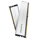
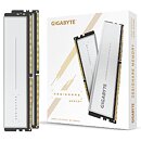
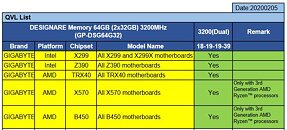
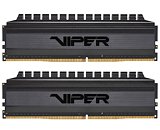
GIGABYTE expanded its teething DDR4 memory lineup with a new 16 GB (2x 8 GB) dual-channel DDR4 memory kit, called simply "GIGABYTE Memory 2666MHz." These modules lack the Aorus branding featured on the company's very first DDR4 modules. You instead get 32 mm tall, 7 mm-thick modules with a restrained design, and plain GIGABYTE branding.

One area where the company refined its design is the heatspreaders, which are thicker, and have more mass to them, even if they lack finnage. GIGABYTE's module does what it says on the tin - DDR4-2666 with 16-16-16-35 timings, at 1.2 Volts. Out of the box, it packs both JEDEC and XMP SPD profiles. Memory controllers that support DDR4-2666 (such as Intel "Coffee Lake" and later), should run it at the advertised speeds without any user intervention. For older platforms, an XMP 2.0 profile helps achieve the advertised settings. The modules are backed by lifetime warranty.

ATP Announces eMMC 5.1 Chips

Fueled by continuous big data generation, the ongoing industrial revolution requires storage solutions that offer not only high performance, but also uncompromising reliability and maximum endurance. ATP Electronics, a leading manufacturer of industrial memory and storage solutions, tackles these tough storage demands with its new industrial e.MMC product family.

The ATP industrial e.MMC, which adheres to JEDEC e.MMC v5.1 Standard (JESD84-B51), is poised to make its mark at the Flash Memory Summit 2018 in Santa Clara, USA from August 7 to 9, 2018.

ATP Miniature Storage Powerhouses Take Center Stage at FMS 2018

The volume of data traffic is growing by the minute, and ATP Electronics, a leading manufacturer of high-performance industrial memory and storage solutions, is meeting colossal storage demands with its latest portfolio built for space-restricted embedded, industrial, and automotive systems. ATP shows off its extensive array of flash memory and storage products at the Flash Memory Summit 2018 in Sta. Clara, USA from August 7 to 9.

"We are seeing data propelling the transformation of cities and nations, and we need effective solutions of handling, storing and analyzing data to deliver rapid, actionable insights that will improve the way we live and do business," noted Marco Mezger, ATP Vice President of Global Marketing. "As the Internet of Things (IoT) adoption gains momentum, systems are diminishing in size so memory and storage solutions have to adapt. ATP is thoroughly amplifying reliability, endurance, performance and capacity in its embedded and removable flash products while keeping them compact and portable," he added.

INNOVENTIONS Launches Memory Testers for DDR4

INNOVENTIONS, Inc., the leading manufacturer of portable computer memory testers, is now shipping the RAMCHECK LX DDR4 and the RAMCHECK LX DDR4 Pro for testing and identifying industry standard DDR4 ECC and non-ECC SDRAM modules.

"DDR4 memory is now the standard for servers and PCs," said Dr. David Y. Feinstein, President of INNOVENTIONS. "With these new RAMCHECK LX memory testers, data centers, memory dealers and repair techs have a great tool to test and identify DDR4 DIMMs quickly and reliably. Considering the price of these big server DIMMs, the RAMCHECK LX pays for itself pretty quickly."

JEDEC Publishes Universal Flash Storage (UFS & UFSHCI) v3.0 and UFS Card v1.1

JEDEC Solid State Technology Association, the global leader in the development of standards for the microelectronics industry, today announced the publication of Universal Flash Storage (UFS) version 3.0, JESD220D. In addition, new updates to related standards, JESD223D UFSHCI and JESD220-2A UFS Card Extension, have also been published. Developed for mobile applications and computing systems requiring high performance with low power consumption, UFS 3.0 is the first standard to introduce MIPI M-PHY HS-Gear4, with a data rate of up to 11.6 Gbps per lane, a 2x performance increase over prior versions of the specification. UFS 3.0 includes two features introduced specifically for the automotive market: the ability to function at an extended temperature range and refresh operation. JESD220D, JESD223D and JESD220-2A are available for download from the JEDEC website.

UFS is a high-performance interface designed for use in applications where power consumption needs to be minimized, including mobile systems such as smart phones and tablets as well as automotive applications. Its high-speed serial interface and optimized protocol enable significant improvements in throughput and system performance.

To achieve the highest performance and most power efficient data transport, JEDEC UFS leverages industry leading specifications from the MIPI Alliance to form its Interconnect Layer. This collaboration continues with UFS version 3.0, which references the MIPI M-PHY v4.1 physical layer specification and the recently released MIPI UniProSM v1.8 transport layer specification.

Greenliant Expands Portfolio of eMMC NANDrive

Greenliant Systems is now sampling its eMMC 5.1 NANDrive embedded solid state drive (SSD) product family with improved performance, enhanced features and a wide range of capacities (8, 16, 32, 64 and 128 GB). Ideal for automotive, industrial, medical, security, military and networking applications, the new GLS85VM NANDrive devices support the JEDEC eMMC 5.1 standard and operate at full industrial temperatures between -40 and +85 degrees Celsius.

The eMMC 5.1 NANDrive products are HS200/HS400 compliant and support command queuing for faster data throughput and better multitasking. These high-performance products also offer high-reliability features, such as advanced wear-leveling, bad block management and effective error correction code (ECC) capabilities to significantly extend the life of the product. eMMC 5.1 NANDrive SSDs are available in a 14mm x 18mm, 100-ball, 1.0mm pitch package (backward compatible with Greenliant's 100-ball eMMC 4.4 NANDrive SSDs) and will also be offered in a smaller 11.5mm x 13mm, 153-ball, 0.5mm pitch package.

Toshiba Unveils Embedded NAND Flash Memory Products for Automotive Applications

Toshiba Memory Corporation, the world leader in memory solutions, today announced that it has begun shipping samples of embedded NAND flash memory products for automotive applications that are compliant with JEDEC UFS version 2.1. The new products meet AEC-Q100 Grade2 requirements and support a wide temperature range of -40°C to +105°C, offering the enhanced reliability capabilities that are required by increasingly complex automotive applications. The line-up meets a broad range of applications requirements with five different capacities: 16 GB, 32 GB, 64 GB, 128 GB and 256 GB.

The new products are embedded NAND flash memory products that integrate NAND chips fabricated with 15 nm process technology and a controller in a single package. Storage requirements for automotive applications continue to increase as systems including automotive information & entertainment systems and ADAS become more sophisticated, and UFS supports their high performance and density needs. The addition of automotive UFS expands Toshiba Memory Corporation's line-up of embedded NAND flash memory products for automotive applications, which currently includes automotive e-MMC products. Utilizing the UFS interface allows the new products to achieve sequential read of 850 MB/s and random read of 50,000 IOPS, which are approximately 2.7 times and 7.1 times faster than their current e-MMC counterparts, respectively.

Toshiba Memory Unveils UFS Devices Utilizing 64-Layer 3D Flash

Toshiba Memory Corporation, the world leader in memory solutions, has today started sampling Universal Flash Storage (UFS) devices utilizing Toshiba Memory Corporation's cutting-edge 64-layer, BiCS FLASH 3D flash memory. The new UFS devices meet performance demands for applications that require high-speed read/write performance and low power consumption, including mobile devices such as smartphones and tablets, and augmented and virtual reality systems.

The new line-up will be available in four capacities: 32 GB, 64 GB, 128 GB and 256 GB. All of the devices integrate flash memory and a controller in a single, JEDEC-standard 11.5 x 13 mm package. The controller performs error correction, wear leveling, logical-to-physical address translation and bad-block management, allowing users to simplify system development.

Kingmax Announces the Zeus Dragon DDR4 Memory Series

Kingmax, a memory expert, released Zeus Dragon DDR4 on November 13, 2017. This is made for gamers and DIY enthusiasts. The innovative design is integrated with aesthetics and functions which amazes everyone. Gamers can enjoy its appearance and function.

Zeus Dragon DDR4 uses aluminum alloy heat sink to effectively emit heat, therefore protecting memory and extending the service life. Zeus Dragon uses the dragon symbol blending both Eastern and Western style. The luxurious etchings present the superiority of the dragon and display the assertiveness and dignity of royalty. The dragon is above all other creatures and has extraordinary power and stunning speed. Besides its shiny scales, its powerful magic is neck and neck when it fights against Zeus, the ruler of all gods, in order to protect treasure.

Samsung Starts Producing UFS for Automotive Applications

Samsung Electronics Co., Ltd., the world leader in advanced memory technology, today announced that it is introducing the industry's first embedded Universal Flash Storage (eUFS) solution for use in next-generation automotive applications. Consisting of 128-gigabyte (GB) and 64GB versions, the new eUFS solution has been designed for advanced driver-assistance systems (ADAS), next-generation dashboards and infotainment systems that provide comprehensive connected features for drivers and passengers worldwide.

"We are taking a major step in accelerating the introduction of next-generation ADAS and automotive infotainment systems by offering the industry's first eUFS solution for the market much earlier than expected," said Jinman Han, senior vice president of Memory Product Planning & Application Engineering at Samsung Electronics. "Samsung is taking the lead in the growth of the memory market for sophisticated automotive applications, while continuing to deliver leading-edge UFS solutions with higher performance, density and reliability."

Rambus Has DDR5 Memory Working in Its Labs, Gears for 2019 Market Release

DDR5, the natural successor to today's DDR4 memory that brings with double the bandwidth and density versus current generation DDR4. along with delivering improved channel efficiency, is expected to be available in the market starting 2019. JEDEC, the standards body responsible for the DDR specifications, says that base DDR5 frequencies should be at around DDR5-4800 - more than double that of base DDR4's 2133, but a stone throw away from today's fastest (and uber, kidney-like-expensive) 4600 MHz memory kits from the likes of G.Skill and Corsair.

DDR5 is expected to support data rates up to 6.4 Gb/s delivering 51.2 GB/s max, up from 3.2 Gb/s and 25.6 GB/s for today's DDR4. The new version will push the 64-bit link down to 1.1V and burst lengths to 16 bits from 1.2V and 8 bits. In addition, DDR5 lets voltage regulators ride on the memory card rather than the motherboard. CPU vendors are also expected to expand the number of DDR channels on their processors from 12 to 16, which could drive main memory sizes to 128 GB from 64 GB today. Whether this will be good for end-users in relation to DDR5 memory prices remains open for debate; however, considering the rampant memory prices this side of 2017, chances are it won't be unless supply increases considerably.

SK Hynix Announces its 8Gb GDDR6 Memory Chips

SK Hynix Inc. today introduced the world's fastest 2Znm 8Gb (Gigabit) GDDR6 (Graphics DDR6) DRAM. The product operates with an I/O data rate of 16 Gbps (Gigabits per second) per pin, which is the industry's fastest. With a forthcoming high-end graphics card of 384-bit I/Os, this DRAM processes up to 768 GB/s (Gigabytes of graphics data per second). SK Hynix has been planning to mass produce the product for a client to release high-end graphics card by early 2018 equipped with high performance GDDR6 DRAMs.

GDDR is specialized DRAM for processing an extensive amount of graphics data quickly according to what graphics cards command in PCs, workstations, video players and high performance gaming machines. Especially, GDDR6 is a next generation graphics solution under development of standards at JEDEC, which runs twice as fast as GDDR5 having 10% lower operation voltage. As a result, it is expected to speedily substitute for GDDR5 and GDDR5X. SK Hynix has been collaborating with a core graphics chipset client to timely mass produce the GDDR6 for the upcoming market demands.

JEDEC Says DDR5 Standard Development Rapidly Advancing: ETA, 2018

JEDEC Solid State Technology Association, responsible for creating the standards on which all of your versions of DDR memory are based upon, recently announced that development of the DDR5 memory standard is well underway, and in time for a 2018 release. The standards body said DDR5 memory will provide double the bandwidth and density versus current generation DDR4. along with delivering improved channel efficiency. Though considering the rate at which DDR4 prices have been increasing as of late, we really should fell a little uneasy at what this new memory standard's adoption will entail.

The current highest base clock that JEDEC allows in their DDR4 memory standard before "overclocking" takes over is DDR4-2400 - with timings ranging from 15~18 for the CAS latency, as well as tRCD, and tRP. And if, as JEDEC says, DDR5 is to be "twice as fast", that could imply that we could end up seeing DDR5-4800. Consider that for a moment: DDR4 kits today only go so far as DDR4-4266, and those are so few and far between that they'll cost you a singular kidney.

Rambus Introduces High Bandwidth Memory PHY on GlobalFoundries FX-14

Rambus Inc. today announced the availability of its High Bandwidth Memory (HBM) Gen2 PHY developed for GLOBALFOUNDRIES high-performance FX-14 ASIC Platform. Built on the GLOBALFOUNDRIES 14nm FinFET (14LPP) process technology, the Rambus HBM PHY is aimed at networking and data center applications and designed for systems that require low latency and high bandwidth memory. This PHY is fully compliant with the JEDEC HBM2 standard and supports data rates up to 2000 Mbps per data pin, enabling a total bandwidth of 256 GB/s to meet the needs of today's most data-intensive tasks.

"Data center needs are continuously changing and we are at the forefront of delivering memory interface technology designed to meet today's most demanding workloads," said Luc Seraphin, senior vice president and general manager of the Rambus Memory and Interfaces division. "Through our collaboration with GLOBALFOUNDRIES, we are delivering a comprehensive and robust solution for high-performance data center and networking applications. Our HBM offering will allow data center solution developers to bring high performance memory closer to the CPU, thus reducing latency and improving the system throughput."

InnoDisk Intros DDR4-2666 Memory for Server on Upcoming Purley Platform

Innodisk, the service driven flash and DRAM provider, introduces the new DDR4 2666 memory modules designed for server applications on the upcoming Purley platform that Intel intends to release in 2017. The DDR4 2666 RDIMM is equipped with a Samsung chip which is designed with a new system circuit architecture to deliver even higher performance with lower power consumption.

"For years, Innodisk has been dedicated to developing and manufacturing industrial grade memory modules, and we have never stopped introducing industry leading products," said Samson Chang, Vice President of Embedded DRAM Business Unit of Innodisk. "We are proud to introduce the industry's first DDR4 RDIMM with an initial speed 2666 MT/s. It will optimize the Purley platform and maximize its performance. Innodisk will continue to develop more advanced product specifications in the future, allowing us to have the most complete product line amongst our competitors. Our goal is to support our customers various needs and lead the industrial systems upgrade."

Toshiba Announces New-Generation Supreme+ eMMC Flash Storage

Toshiba America Electronic Components, Inc. (TAEC) has enhanced its lineup of managed NAND devices with the addition of new Embedded Multimedia Card (e-MMC) and Universal Flash Storage (UFS) embedded memory solutions. Featuring enhanced integrated controller technologies, the new 'Supreme+' e-MMC (JEDEC ver. 5.1) and UFS (JEDEC ver. 2.1) offerings deliver significant read and write speed improvements to demanding applications.

In contrast to raw NAND flash memory solutions, e-MMC and UFS devices integrate NAND flash memory and a controller chip in a single package. This saves space and relieves host processors of the burden of key memory management functions including bad block management, error correction, wear leveling, and garbage collection. As a result, e-MMC and UFS devices simplify design when compared to standalone memory ICs with a standard NAND flash interface.

Samsung Also Unveils a 256 GB UFS Card

Samsung Electronics Co., Ltd., the world leader in advanced memory technology, today unveiled the industry's first removable memory cards based on the JEDEC Universal Flash Storage (UFS) 1.0 Card Extension Standard*, for use in high-resolution mobile shooting devices such as DSLRs, 3D VR cameras, action cams and drones. Coming in a wide range of storage capacities including 256, 128, 64 and 32 gigabyte (GB), Samsung's UFS cards are expected to bring a significant performance boost to the external memory storage market, allowing much more satisfying multimedia experiences.

"Our new 256GB UFS card will provide an ideal user experience for digitally-minded consumers and lead the industry in establishing the most competitive memory card solution," said Jung-bae Lee, senior vice president, Memory Product Planning & Application Engineering, Samsung Electronics "By launching our new high-capacity, high-performance UFS card line-up, we are changing the growth paradigm of the memory card market to prioritize performance and user convenience above all."

JEDEC Updates Universal Flash Storage (UFS) and Related Standards

JEDEC Solid State Technology Association, the global leader in the development of standards for the microelectronics industry, today announced the publication of several key updates to the Universal Flash Storage (UFS) family of standards. These include JESD220C UFS version 2.1, JESD223C UFSHCI version 2.1, JESD220-1A UFS UME version 1.1 and JESD223-1A UFSHCI UME version 1.1.

Developed for mobile applications and computing systems requiring high performance with low power consumption, the new UFS updates offer key improvements over earlier versions which will provide data security through the use of inline cryptography between the SoC and UFS Storage device. All four updated standards are available for free download from the JEDEC website.

JEDEC Publishes Universal Flash Storage (UFS) Removable Card Standard

JEDEC Solid State Technology Association, the global leader in the development of standards for the microelectronics industry, today announced the publication of JESD220-2 Universal Flash Storage (UFS) Card Extension Standard. The new removable memory card standard standardizes functionality that aligns with the popular UFS embedded device standard. JESD220-2 is available for free download from the JEDEC website.

UFS is a high performance interface designed for use in computing and mobile systems such as smart phones and tablets where power consumption needs to be minimized. Its high speed serial interface and optimized protocol enable significant improvements in throughput and mobile system performance. The new UFS card standard provides a leading-edge removable storage solution while maintaining sequential and random IOPS performance that is critical for future mobile markets. Even using a single lane the UFS 1.0 card offers 600 MB/s interface speed in both directions and a state-of-the-art queuing mechanism to further increase system throughput.

JEDEC Announces Publication of GDDR5X Graphics Memory Standard

JEDEC Solid State Technology Association, the global leader in the development of standards for the microelectronics industry, today announced the publication of JESD232 Graphics Double Data Rate (GDDR5X) SGRAM. Available for free download from the JEDEC website, the new memory standard is designed to satisfy the increasing need for more memory bandwidth in graphics, gaming, compute, and networking applications.

Derived from the widely adopted GDDR5 SGRAM JEDEC standard, GDDR5X specifies key elements related to the design and operability of memory chips for applications requiring very high memory bandwidth. With the intent to address the needs of high-performance applications demanding ever higher data rates, GDDR5X is targeting data rates of 10 to 14 Gb/s, a 2X increase over GDDR5. In order to allow a smooth transition from GDDR5, GDDR5X utilizes the same, proven pseudo open drain (POD) signaling as GDDR5.

"GDDR5X represents a significant leap forward for high end GPU design," said Mian Quddus, JEDEC Board of Directors Chairman. "Its performance improvements over the prior standard will help enable the next generation of graphics and other high-performance applications."

JEDEC Updates Groundbreaking High Bandwidth Memory (HBM) Standard

JEDEC Solid State Technology Association, the global leader in the development of standards for the microelectronics industry, today announced the publication of an update to JESD235 High Bandwidth Memory (HBM) DRAM standard. HBM DRAM is used in Graphics, High Performance Computing, Server, Networking and Client applications where peak bandwidth, bandwidth per watt, and capacity per area are valued metrics to a solution's success in the market. The standard was developed and updated with support from leading GPU and CPU developers to extend the system bandwidth growth curve beyond levels supported by traditional discrete packaged memory. JESD235A is available for free download from the JEDEC website.

JESD235A leverages Wide I/O and TSV technologies to support up to 8 GB per device at speeds up to 256 GB/s. This bandwidth is delivered across a 1024-bit wide device interface that is divided into 8 independent channels on each DRAM stack. The standard supports 2-high, 4-high and 8-high TSV stacks of DRAM at full bandwidth to allow systems flexibility on capacity requirements from 1 GB - 8 GB per stack.
Return to Keyword Browsing
Jul 15th, 2024 22:48 EDT change timezone

New Forum Posts

Popular Reviews

Controversial News Posts