News Posts matching #N5

Return to Keyword Browsing

Fujitsu Previews Monaka: 144-Core Arm CPU Made with Chiplets

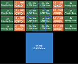
Fujitsu has previewed its next-generation Monaka processor, a 144-core powerhouse for data center. Satoshi Matsuoka of the RIKEN Center for Computational Science showcased the mechanical sample on social media platform X. The Monaka processor is developed in collaboration with Broadcom and employs an innovative 3.5D eXtreme Dimension System-in-Package architecture featuring four 36-core chiplets manufactured using TSMC's N2 process. These chiplets are stacked face-to-face with SRAM tiles through hybrid copper bonding, utilizing TSMC's N5 process for the cache layer. A distinguishing feature of the Monaka design is its approach to memory architecture. Rather than incorporating HBM, Fujitsu has opted for pure cache dies below compute logic in combination with DDR5 DRAM compatibility, potentially leveraging advanced modules like MR-DIMM and MCR-DIMM.

The processor's I/O die supports cutting-edge interfaces, including DDR5 memory, PCIe 6.0, and CXL 3.0 for seamless integration with modern data center infrastructure. Security in the design is taken care of with the implementation of Armv9-A's Confidential Computing Architecture for enhanced workload isolation. Fujitsu has set ambitious goals for the Monaka processor. The company aims to achieve twice the energy efficiency of current x86 processors by 2027 while maintaining air cooling capabilities. The processor aims to do AI and HPC with the Arm SVE 2 support, which enables vector lengths up to 2048 bits. Scheduled for release during Fujitsu's fiscal year 2027 (April 2026 to March 2027), the Monaka processor is shaping up as a competitor to AMD's EPYC and Intel's Xeon processors.

Kioxia Develops OCTRAM (Oxide-Semiconductor Channel Transistor DRAM) Technology

Kioxia Corporation, a world leader in memory solutions, today announced the development of OCTRAM (Oxide-Semiconductor Channel Transistor DRAM), a new type of 4F2 DRAM, comprised of an oxide-semiconductor transistor that has a high ON current, and an ultra-low OFF current, simultaneously. This technology is expected to realize a low power DRAM by bringing out the ultra-low leakage property of the InGaZnO transistor. This was first announced at the IEEE International Electron Devices Meeting (IEDM) held in San Francisco, CA on December 9, 2024. This achievement was jointly developed by Nanya Technology and Kioxia Corporation. This technology has the potential to lower power consumption in a wide range of applications, including AI and post-5G communication systems, and IoT products.

The OCTRAM utilizes a cylinder-shaped InGaZnO vertical transistor (Fig.1) as a cell transistor. This design enables the adaptation of a 4F2 DRAM, which offers significant advantages in memory density compared to the conventional silicon-based 6F2 DRAM.

TSMC Could Bring 2 nm Production Overseas, Taiwanese Minister Confirms

Taiwanese political officials have agreed to discuss transferring TSMC's advanced 2 nm chip technology to allied democratic nations, but only after establishing the main mass production launch in late 2025 in Taiwan. This new stance comes amid growing international pressure and recent comments from upcoming US president Donald Trump about semiconductor manufacturing. The announcement by National Science and Technology Council Minister Cheng-Wen Wu marks a notable departure from earlier statements by Economic Affairs Minister J.W. Kuo, who had previously emphasized legal restrictions on transferring leading-edge process technology overseas. Interestingly, these different positions aren't so different from one point: timeline of node deployments. As TSMC produces latest nodes in Taiwan, overseas production will lag by a generation or two.

TSMC plans to implement its 2 nm technology in US facilities by 2030. The company's Arizona facility, Fab 21, will begin with less advanced N4 and N5 processes in early 2025 and progress to 3 nm technology by 2028. However, this timeline could face pressure for acceleration, mainly if new trade policies are implemented. Industry analyst Dan Nystedt points out significant challenges in transferring advanced chip production. Integrating research and development with manufacturing processes in Taiwan provides crucial advantages for initial production ramps, making simultaneous mass production launches in multiple locations technically challenging. Simply put, there aren't enough capable engineers, scientists, and factory workers capable of doing what TSMC accomplishes in Taiwan.

AMD Ryzen AI MAX 300 "Strix Halo" iGPU to Feature Radeon 8000S Branding

AMD Ryzen AI MAX 300-series processors, codenamed "Strix Halo," have been on in the news for close to a year now. These mobile processors combine "Zen 5" CPU cores with an oversized iGPU that offers performance rivaling discrete GPUs, with the idea behind these chips being to rival the Apple M3 Pro and M3 Max processors powering MacBook Pros. The "Strix Halo" mobile processor is an MCM that combines one or two "Zen 5" CCDs (some ones featured on "Granite Ridge" desktop processors and "Turin" server processors), with a large SoC die. This die is built either on the 5 nm (TSMC N5) or 4 nm (TSMC N4P) node. It packs a large iGPU based on the RDNA 3.5 graphics architecture, with 40 compute units (CU), and a 50 TOPS-class XDNA 2 NPU carried over from "Strix Point." The memory interface is a 256-bit wide LPDDR5X-8000 for sufficient memory bandwidth for the up to 16 "Zen 5" CPU cores, the 50 TOPS NPU, and the large 40 CU iGPU.

Golden Pig Upgrade leaked what looks like a company slide from a notebook OEM, which reveals the iGPU model names for the various Ryzen AI MAX 300-series SKUs. Leading the pack is the Ryzen AI MAX+ 395. This is a maxed out SKU with a 16-core/32-thread "Zen 5" CPU that uses two CCDs. All 16 cores are full-sized "Zen 5." The CPU has 64 MB of L3 cache (32 MB per CCD), each of the 16 cores has 1 MB of dedicated L2 cache. The iGPU is branded Radeon 8060S, it comes with all 40 CU (2,560 stream processors) enabled, besides 80 AI accelerators, and 40 Ray accelerators. The Ryzen AI MAX 390 is the next processor SKU, it comes with a 12-core/24-thread "Zen 5" CPU. Like the 395, the 390 is a dual-CCD processor, all 12 cores are full-sized "Zen 5." There's 64 MB of L3 cache, and 1 MB of L2 cache per core. The Radeon 8060S graphics solution is the same as the one on the Ryzen AI MAX+ 395, it comes with all 40 CU enabled.

Credo Announces PCI Express 6/7, Compute Express Link CXL 3.x Retimers, and AEC PCI Express Product Line at OCP Summit 2024

Credo Technology Group Holding Ltd (Credo), an innovator in providing secure, high-speed connectivity solutions that deliver improved energy efficiency as data rates and corresponding bandwidth requirements increase throughout the data infrastructure market, is excited to announce the company's first Toucan PCI Express (PCIe) 6, Compute Express Link (CXL) 3.x and Magpie PCIe 7, CXL 4.x retimers and OSFP-XD 16x 64GT/s (1 Tb) PCIe 6/CXL HiWire AECs. Credo will demonstrate the Toucan PCIe 6 retimers and HiWire AECs at the upcoming Open Compute Project (OCP) Summit October 15-17 in Booth 31 and the OCP Innovation Center.

Building on Credo's renowned Serializer/Deserializer (SerDes) technology, the new PCIe 6 and PCIe 7 retimers deliver industry-leading performance and power efficiency while being built on lower cost, more mature process nodes than competing devices. Credo will also include enhanced diagnostic tools, including an embedded logic analyzer and advanced SerDes tools driven by a new GUI designed to enable rapid bring up and debug of customer systems.

AMD Granite Ridge "Zen 5" Processor Annotated

High-resolution die-shots of the AMD "Zen 5" 8-core CCD were released and annotated by Nemez, Fitzchens Fitz, and HighYieldYT. These provide a detailed view of how the silicon and its various components appear, particularly the new "Zen 5" CPU core with its 512-bit FPU. The "Granite Ridge" package looks similar to "Raphael," with up to two 8-core CPU complex dies (CCDs) depending on the processor model, and a centrally located client I/O die (cIOD). This cIOD is carried over from "Raphael," which minimizes product development costs for AMD at least for the uncore portion of the processor. The "Zen 5" CCD is built on the TSMC N4P (4 nm) foundry node.

The "Granite Ridge" package sees the up to two "Zen 5" CCDs snuck up closer to each other than the "Zen 4" CCDs on "Raphael." In the picture above, you can see the pad of the absent CCD behind the solder mask of the fiberglass substrate, close to the present CCD. The CCD contains 8 full-sized "Zen 5" CPU cores, each with 1 MB of L2 cache, and a centrally located 32 MB L3 cache that's shared among all eight cores. The only other components are an SMU (system management unit), and the Infinity Fabric over Package (IFoP) PHYs, which connect the CCD to the cIOD.

Synopsys and TSMC Pave the Path for Trillion-Transistor AI and Multi-Die Chip Design

Synopsys, Inc. today announced its continued, close collaboration with TSMC to deliver advanced EDA and IP solutions on TSMC's most advanced process and 3DFabric technologies to accelerate innovation for AI and multi-die designs. The relentless computational demands in AI applications require semiconductor technologies to keep pace. From an industry leading AI-driven EDA suite, powered by Synopsys.ai for enhanced productivity and silicon results to complete solutions that facilitate the migration to 2.5/3D multi-die architectures, Synopsys and TSMC have worked closely for decades to pave the path for the future of billion to trillion-transistor AI chip designs.

"TSMC is excited to collaborate with Synopsys to develop pioneering EDA and IP solutions tailored for the rigorous compute demands of AI designs on TSMC advanced process and 3DFabric technologies," said Dan Kochpatcharin, head of the Ecosystem and Alliance Management Division at TSMC. "The results of our latest collaboration across Synopsys' AI-driven EDA suite and silicon-proven IP have helped our mutual customers significantly enhance their productivity and deliver remarkable performance, power, and area results for advanced AI chip designs.

Broadcom's Testing of Intel 18A Node Signals Disappointment, Still Not Ready for High-Volume Production

According to a recent Reuters report, Intel's 18A node doesn't seem to be production-ready. As the sources indicate, Broadcom has been reportedly testing Intel's 18A node on its internal company designs, which include an extensive range of products from AI accelerators to networking switches. However, as Broadcom received the initial production run from Intel, the 18A node seems to be in a worse state than initially expected. After testing the wafers and powering them on, Broadcom reportedly concluded that the 18A process is not yet ready for high-volume production. With Broadcom's comments reflecting high-volume production, it signals that the 18A node is not producing a decent yield that would satisfy external customers.

While this is not a good sign of Intel's Fundry contract business development, it shows that the node is presumably in a good state in terms of power/performance. Intel's CEO Pat Gelsinger confirmed that 18A is now at 0.4 d0 defect density, and it is now a "healthy process." However, alternatives exist at TSMC, which proves to be a very challenging competitor to take on, as its N7 and N5 nodes had a defect density of 0.33 during development and 0.1 defect density during high-volume production. This leads to better yields and lower costs for the contracting party, resulting in higher profits. Ultimately, it is up to Intel to improve its production process further to satisfy customers. Gelsinger wants to see Intel Foundry as "manufacturing ready" by the end of the year, and we can see the first designs in 2025 reach volume production. There are still a few more months to improve the node, and we expect to see changes implemented by the end of the year.

Ryzen 9000 Chip Layout: New Details Announced

AMD "Granite Ridge" is codename for the four new Ryzen 9000 series desktop processors the company plans to launch on July 31, 2024. The processor is built in the Socket AM5 package, and is meant to be backwards compatible with AMD 600-series chipset motherboards, besides the new 800-series chipset ones that will launch alongside. "Granite Ridge" is a chiplet-based processor, much like the Ryzen 7000 "Raphael," Ryzen 5000 "Vermeer," and Ryzen 3000 "Matisse." AMD is carrying over the 6 nm client I/O die over from "Raphael" in an effort to minimize development costs, much in the same way it carried over the 12 nm cIOD for "Vermeer" from "Matisse."

The SoC I/O features of "Granite Ridge" are contemporary, with its awesome 28-lane PCI-Express Gen 5 root complex that allows a PCI-Express 5.0 x16, two CPU-attached M.2 Gen 5 slots, and a Gen 5 x4 chipset bus. There's also a basic integrated graphics solution based on the older RDNA 2 graphics architecture; which should make these processors fit for all use-cases that don't need discrete graphics. The iGPU even has multimedia accelerators, an audio coprocessor, a display controller, and USB 3.2 interfaces from the processor.

TSMC Unveils Next-Generation HBM4 Base Dies, Built on 12 nm and 5 nm Nodes

During the European Technology Symposium 2024, TSMC has announced its readiness to manufacture next-generation HBM4 base dies using both 12 nm and 5 nm nodes. This significant development is expected to substantially improve the performance, power consumption, and logic density of HBM4 memory, catering to the demands of high-performance computing (HPC) and artificial intelligence (AI) applications. The shift from a traditional 1024-bit interface to an ultra-wide 2048-bit interface is a key aspect of the new HBM4 standard. This change will enable the integration of more logic and higher performance while reducing power consumption. TSMC's N12FFC+ and N5 processes will be used to produce these base dies, with the N12FFC+ process offering a cost-effective solution for achieving HBM4 performance and the N5 process providing even more logic and lower power consumption at HBM4 speeds.

The company is collaborating with major HBM memory partners, including Micron, Samsung, and SK Hynix, to integrate advanced nodes for HBM4 full-stack integration. TSMC's base die, fabricated using the N12FFC+ process, will be used to install HBM4 memory stacks on a silicon interposer alongside system-on-chips (SoCs). This setup will enable the creation of 12-Hi (48 GB) and 16-Hi (64 GB) stacks with per-stack bandwidth exceeding 2 TB/s. TSMC's collaboration with EDA partners like Cadence, Synopsys, and Ansys ensures the integrity of HBM4 channel signals, thermal accuracy, and electromagnetic interference (EMI) in the new HBM4 base dies. TSMC is also optimizing CoWoS-L and CoWoS-R for HBM4 integration, meaning that massive high-performance chips are already utilizing this technology and getting ready for volume manufacturing.

TSMC to Introduce Location Premium for Overseas Chip Production

As a part of its Q1 earnings call discussion, one of the largest semiconductor manufacturers, TSMC, has unveiled a strategic move to charge a premium for chips manufactured at its newly established overseas fabrication plants. During an earnings call, TSMC's CEO, C.C. Wei, announced that the company will impose higher pricing for chips produced outside Taiwan to offset the higher operational costs associated with these international locations. This move aims to maintain TSMC's target gross margin of 53% amidst rising expenses such as inflation and elevated electricity costs. This decision comes as TSMC expands its global footprint with new facilities in the United States, Germany, and Japan (JAMS) to meet the increasing demand for semiconductor chips worldwide. The company's new US-based Arizona facility, known as Fab 21, has faced delays due to equipment installation issues and labor negotiations.

Chips produced at this site, utilizing TSMC's advanced N5 and N4 nodes, could cost between 20% to 30% more than those manufactured in Taiwan. TSMC's strategy to manage the cost disparities across different geographic locations involves strategic pricing, securing government support, and leveraging its manufacturing technology leadership. This approach reflects the company's commitment to maintaining its competitive edge while navigating the complexities of global semiconductor manufacturing in today's fragmented market. Introducing a location premium is expected to impact American semiconductor designers, who may need to pass these costs on to specific market segments, particularly those with lower price sensitivity, such as government-related projects. Despite these challenges, TSMC's overseas expansion underscores its adaptive strategies in the face of global economic pressures and industry demands, ensuring its continued position as a leading player in the semiconductor industry.

AMD 5th Gen EPYC "Turin" Pictured: Who Needs Accelerators When You Have 192 Cores?

AMD's upcoming server processor, the 5th Gen EPYC "Turin," has been pictured as an engineering sample is probably being evaluated by the company's data-center or cloud customers. The processor has a mammoth core-count of 192-core/384-thread in its high-density cloud-focused variant that uses "Zen 5c" CPU cores. Its regular version that uses larger "Zen 5" cores that can sustain higher clock speeds, also comes with a fairly high core-count of 128-core/256-thread, up from the 96-core/192-thread of the "Zen 4" based EPYC "Genoa."

The EPYC "Turin" server processor based on "Zen 5" comes with an updated sIOD (server I/O die), surrounded by as many as 16 CCDs (CPU complex dies). AMD is expected to build these CCDs on the TSMC N4P foundry node, which is a more advanced version of the TSMC N4 node the company currently uses for its "Phoenix" client processors, and the TSMC N5 node it uses for its "Zen 4" CCD. TSMC claims that the N4P node offers an up to 22% improvement in power efficiency over N5, as well as a 6% increase in transistor density. Each of the "Zen 5" CCDs is confirmed to have 8 CPU cores sharing 32 MB L3 cache memory. A total of 16 such CCDs add up to the processor's 128-core/256-thread number. The high-density "Turin" meant for cloud data-centers, is a whole different beast.

MediaTek Successfully Develops First Chip Using TSMC's 3 nm Process, Set for Volume Production in 2024

MediaTek and TSMC today announced that MediaTek has successfully developed its first chip using TSMC's leading-edge 3 nm technology, taping out MediaTek's flagship Dimensity system-on-chip (SoC) with volume production expected next year. This marks a significant milestone in the long-standing strategic partnership between MediaTek and TSMC, with both companies taking full advantage of their strengths in chip design and manufacturing to jointly create flagship SoCs with high performance and low power features, empowering global end devices.

"We are committed to our vision of using the world's most advanced technology to create cutting edge products that improve our lives in meaningful ways," said Joe Chen, President of MediaTek. "TSMC's consistent and high-quality manufacturing capabilities enable MediaTek to fully demonstrate its superior design in flagship chipsets, offering the highest performance and quality solutions to our global customers and enhancing the user experience in the flagship market."

TSMC Holds 3nm Volume Production and Capacity Expansion Ceremony, Marking a Key Milestone for Advanced Manufacturing

TSMC today held a 3 nanometer (3 nm) Volume Production and Capacity Expansion Ceremony at its Fab 18 new construction site in the Southern Taiwan Science Park (STSP), bringing together suppliers, construction partners, central and local government, the Taiwan Semiconductor Industry Association, and members of academia to witness an important milestone in the Company's advanced manufacturing.

TSMC has laid a strong foundation for 3 nm technology and capacity expansion, with Fab 18 located in the STSP serving as the Company's GIGAFAB facility producing 5 nm and 3 nm process technology. Today, TSMC announced that 3 nm technology has successfully entered volume production with good yields, and held a topping ceremony for its Fab 18 Phase 8 facility. TSMC estimates that 3 nm technology will create end products with a market value of US$1.5 trillion within five years of volume production.

TSMC Cuts Back CAPEX Budget Despite Record Profits

Another quarter, another record breaking earnings report by TSMC, but it seems like the company has released that things are set to slow down sooner than initially expected and the company is hitting the brakes on some of its expansion projects. The company saw a 79.7 percent increase in profits compared to last year, with a profit of US$8.8 billion and a revenue of somewhere between US$19.9 to US$ 20.7 billion for the third quarter, which is a 47.9 percent bump compared to last year. TSMC's 5 nm nodes were the source for 28 percent of the revenues, followed by 26 percent for 7 nm nodes, 12 percent for 16 nm and 10 percent for 28 nm, with remaining nodes at 40 nm and larger making up for the remainder of the revenue. By platform, smartphone chips made up 41 percent, followed by High Performance Computing at 39 percent, IoT at 10 percent and automotive at five percent.

TSMC said it will cut back its CAPEX budget by around US$4 billion, to US$36 billion, compared to the earlier stated US$40 billion budget the company had set aside for expanding its fabs. Part of the reason for this is that TSMC is already seeing weaker demand for products manufactured using its N7 and N6 nodes, as the N7 node was meant to be a key part of the new fab in Kaohsiung in southern Taiwan. TSMC is expecting to start production on its first N3 node later this quarter and is expecting the capacity to be fully utilised for all of 2023. Supply is said to be exceeding demand, which TSMC said is partially to blame on tooling delivery issues. TSMC is expecting next year's revenue for its N3 node to be higher than its N5 node in 2020, although the revenue is said to be in the single digit percentage range. The N3E node is said to start production sometime in the second half of next year, or about a quarter earlier than expected. The N2 node isn't due to start production until 2025, but TSMC is already having very high customer engagement, so it doesn't look like TSMC is likely to suffer from a lack of business in the foreseeable future, as long as the company keeps delivering new nodes as planned.

TSMC (Not Intel) Makes the Vast Majority of Logic Tiles on Intel "Meteor Lake" MCM

Intel's next-generation "Meteor Lake" processor is the first mass-production client processor to embody the company's IDM 2.0 manufacturing strategy—one of building processors with multiple logic tiles interconnected with Foveros and a base-tile (essentially an interposer). Each tile is built on a silicon fabrication process most suitable to it, so that the most advanced node could be reserved for the component that benefits from it the most. For example, while you need the SIMD components of the iGPU to be built on an advanced low-power node, you don't need its display controller and media engine to, and these could be relegated to a tile built on a less advanced node. This way Intel is able to maximize its use of wafers for the most advanced nodes in a graded fashion.

Japanese tech publication PC Watch has annotated the "Meteor Lake" SoC, and points out that the vast majority of the chip's tiles and logic die-area is manufactured on TSMC nodes. The MCM consists of four logic tiles—the CPU tile, the Graphics tile, the SoC tile, and the I/O tile. The four sit on a base tile that facilitates extreme-density microscopic wiring interconnecting the logic tiles. The base tile is built on the 22 nm HKMG silicon fabrication node. This tile lacks any logic, and only serves to interconnect the tiles. Intel has an active 22 nm node, and decided it has the right density for the job.

TSMC First Quarter 2022 Financials Show 45.1% Increase in Revenues

A new quarter and another forecast shattering revenue report from TSMC, as the company beat analysts' forecasts by over US$658 million, with a total revenue for the quarter of US$17.6 billion and a net income of almost US$7.26 billion. That's an increase in net income of 45.1 percent or 35.5 percent in sales. Although the monetary figures might be interesting to some, far more interesting details were also shared, such as production updates about future nodes. As a followup on yesterday's news post about 3 nanometer nodes, the N3 node is officially on track for mass production in the second half of this year. TSMC says that customer engagement is stronger than at the start of its N7 and N7 nodes, with HPC and smartphone chip makers lining up to get onboard. The N3E node is, as reported yesterday, expected to enter mass production in the second half of 2023, or a year after N3. Finally, the N2 node is expected in 2025 and won't adhere to TSMC's two year process technology cadence.

Breaking down the revenue by nodes, N7 has taken back the lead over N5, as N7 accounted for 30 percent of TSMC's Q1 revenues up from 27 percent last quarter, but down from 35 percent in the previous year. N5 sits at 20 percent, which is down from 23 percent in the previous quarter, but up from 14 percent a year ago. The 16 and 28 nm nodes still hold on to 25 percent of TSMC's revenue, which is the same as a year ago and up slightly from the previous quarter. Remaining nodes are unchanged from last quarter.

"Navi 31" RDNA3 Sees AMD Double Down on Chiplets: As Many as 7

Way back in January 2021, we heard a spectacular rumor about "Navi 31," the next-generation big GPU by AMD, being the company's first logic-MCM GPU (a GPU with more than one logic die). The company has a legacy of MCM GPUs, but those have been a single logic die surrounded by memory stacks. The RDNA3 graphics architecture that the "Navi 31" is based on, sees AMD fragment the logic die into smaller chiplets, with the goal of ensuring that only those specific components that benefit from the TSMC N5 node (6 nm), such as the number crunching machinery, are built on the node, while ancillary components, such as memory controllers, display controllers, or even media accelerators, are confined to chiplets built on an older node, such as the TSMC N6 (6 nm). AMD had taken this approach with its EPYC and Ryzen processors, where the chiplets with the CPU cores got the better node, and the other logic components got an older one.

Greymon55 predicts an interesting division of labor on the "Navi 31" MCM. Apparently, the number-crunching machinery is spread across two GCD (Graphics Complex Dies?). These dies pack the Shader Engines with their RDNA3 compute units (CU), Command Processor, Geometry Processor, Asynchronous Compute Engines (ACEs), Rendering Backends, etc. These are things that can benefit from the advanced 5 nm node, enabling AMD to the CUs at higher engine clocks. There's also sound logic behind building a big GPU with two such GCDs instead of a single large GCD, as smaller GPUs can be made with a single such GCD (exactly why we have two 8-core chiplets making up a 16-core Ryzen processors, and the one of these being used to create 8-core and 6-core SKUs). The smaller GCD would result in better yields per wafer, and minimize the need for separate wafer orders for a larger die (such as in the case of the Navi 21).

AMD EPYC "Genoa" Zen 4 Processor Multi-Chip Module Pictured

Here is the first picture of a next-generation AMD EPYC "Genoa" processor with its integrated heatspreader (IHS) removed. This is also possibly the first picture of a "Zen 4" CPU Complex Die (CCD). The picture reveals as many as twelve CCDs, and a large sIOD silicon. The "Zen 4" CCDs, built on the TSMC N5 (5 nm EUV) process, look visibly similar in size to the "Zen 3" CCDs built on the N7 (7 nm) process, which means the CCD's transistor count could be significantly higher, given the transistor-density gained from the 5 nm node. Besides more number-crunching machinery on the CPU core, we're hearing that AMD will increase cache sizes, particularly the dedicated L2 cache size, which is expected to be 1 MB per core, doubling from the previous generations of the "Zen" microarchitecture.

Each "Zen 4" CCD is reported to be about 8 mm² smaller in die-area than the "Zen 3" CCD, or about 10% smaller. What's interesting, though, is that the sIOD (server I/O die) is smaller in size, too, estimated to measure 397 mm², compared to the 416 mm² of the "Rome" and "Milan" sIOD. This is good reason to believe that AMD has switched over to a newer foundry process, such as the TSMC N7 (7 nm), to build the sIOD. The current-gen sIOD is built on Global Foundries 12LPP (12 nm). Supporting this theory is the fact that the "Genoa" sIOD has a 50% wider memory I/O (12-channel DDR5), 50% more IFOP ports (Infinity Fabric over package) to interconnect with the CCDs, and the mere fact that PCI-Express 5.0 and DDR5 switching fabric and SerDes (serializer/deserializers), may have higher TDP; which together compel AMD to use a smaller node such as 7 nm, for the sIOD. AMD is expected to debut the EPYC "Genoa" enterprise processors in the second half of 2022.

AMD Ryzen 7000 "Raphael" Zen 4 Processors Enter Mass-Production by April-May?

The next-generation AMD Ryzen 7000 "Raphael" desktop processors in the Socket AM5 package are rumored to enter mass-production soon, according to Greymon55 on Twitter, a reliable source with AMD leaks. Silicon fabrication of the chips may already be underway, as the source claims that packaging (placing the dies on the fiberglass substrate or package), will commence by late-April or early-May. "Raphael" is a multi-chip module of "Zen 4" CCDs fabricated on the TSMC N5 (5 nm) node, combined with a cIOD built on a yet-unknown node. A plant in China performs packaging.

It's hard to predict retail availability, but for the Ryzen 5000 "Vermeer" processors, this development milestone was reached in June 2020, with the first products hitting shelves 4 months later, in November. This was, however, in the thick of the pre-vaccine COVID-19 pandemic. The "Zen 4" CPU cores are expected to introduce an IPC increase, as well as higher clock speeds. Also on offer will be next-gen connectivity, including PCI-Express Gen 5 (including CPU-attached Gen 5 NVMe), and DDR5 memory. These processors will launch alongside Socket AM5 motherboards based on the new AMD 600 series chipsets.

Marvell Introduces Industry's First 800G Multimode Electro-Optics Platform for Cloud Data Centers

Marvell (NASDAQ: MRVL) today announced the industry's first 800 Gbps or 8x 100 Gbps multimode platform solution, that enables data center infrastructure to achieve dramatically higher speeds for short-reach optical modules and Active Optical Cable (AOC) applications. As artificial intelligence (AI), machine learning (ML) and high-performance computing (HPC) applications continue to drive greater bandwidth requirements, cloud-optimized solutions are needed that can bring lower power, latency and cost to short-range data center interconnections. The new 800G platform, which includes Marvell's PAM4 DSP with a multimode transimpedance amplifier (TIA) and Driver, enables faster data center speeds scaling to 800 Gbps, using conventional cost-effective vertical-cavity surface-emitting laser (VCSEL) technology while accelerating time-to-market with plug-and-play deployment.

Today's data centers are packed with equipment utilizing optical modules or AOCs connected by multimode optical fiber optimized for communication over short distances within data centers. This 100G per lane multimode fiber provides cost-effective, low-power, short-reach connectivity. To support multi-gigabit transmissions, multimode architectures often use VCSEL transmitters, which offer the cost benefits of reliability, power efficiency and easy deployment.

Intel Details Ponte Vecchio Accelerator: 63 Tiles, 600 Watt TDP, and Lots of Bandwidth

During the International Solid-State Circuits Conference (ISSCC) 2022, Intel gave us a more significant look at its upcoming Ponte Vecchio HPC accelerator and how it operates. So far, Intel convinced us that the company created Ponte Vecchio out of 47 tiles glued together in one package. However, the ISSCC presentation shows that the accelerator is structured rather interestingly. There are 63 tiles in total, where 16 are reserved for compute, eight are used for RAMBO cache, two are Foveros base tiles, two represent Xe-Link tiles, eight are HBM2E tiles, and EMIB connection takes up 11 tiles. This totals for about 47 tiles. However, an additional 16 thermal tiles used in Ponte Vecchio regulate the massive TDP output of this accelerator.

What is interesting is that Intel gave away details of the RAMBO cache. This novel SRAM technology uses four banks of 3.75 MB groups total of 15 MB per tile. They are connected to the fabric at 1.3 TB/s connection per chip. In contrast, compute tiles are connected at 2.6 TB/s speeds to the chip fabric. With eight RAMBO cache tiles, we get an additional 120 MB SRAM present. The base tile is a 646 mm² die manufactured in Intel 7 semiconductor process and contains 17 layers. It includes a memory controller, the Fully Integrated Voltage Regulators (FIVR), power management, 16-lane PCIe 5.0 connection, and CXL interface. The entire area of Ponte Vecchio is rather impressive, as 47 active tiles take up 2,330 mm², whereas when we include thermal dies, the total area jumps to 3,100 mm². And, of course, the entire package is much larger at 4,844 mm², connected to the system with 4,468 pins.

AMD Readying 16-core "Zen 4" CCDs Exclusively for the Client Segment with an Answer to Intel E-cores?

AMD already declared the CPU core counts of its EPYC "Genoa" and "Bergamo" processors to top out at 96 and 128, respectively, a core-count believed to have been facilitated by the larger fiberglass substrate of the next-gen SP5 CPU socket, letting AMD add more 8-core "Zen 4" chiplets, dubbed CPU complex dies (CCDs). Until now, AMD has used the chiplet as a common component between its EPYC enterprise and Ryzen desktop processors, to differentiate CPU core counts.

A fascinating theory that hit the rumor-mill, indicates that the company might leverage 5 nm (TSMC N5) carve out larger CCDs with up to 16 "Zen 4" CPU cores. Half of these cores are capped at a much lower power budget, essentially making them efficient-cores. This is a concept AMD appears to be carrying over from its 15-Watt class mobile processors, which see the CPU cores operate under an aggressive power-management. These cores still turn out a reasonable amount of performance, and are functionally identical to the ones on 105 W desktop processors with a relaxed power budget.

AMD Socket AM5 "Raphael" Ryzen Processor Confirmed for H2-2022 Launch

AMD's next-generation Ryzen "Raphael" processor could launch only in the second half of 2022, confirms a leaked company slide scored by VideoCardz. The slide points to a Ryzen 5000X3D series product-stack update within the 1H-2022. These are Socket AM4 processors that leverage the company's updated "Zen 3(+)" CPU core die (CCD), which features 64 MB of 3D Vertical cache memory in addition to 32 MB of L3. AMD claims that 3DV Cache technology significantly improves performance akin to a generational update (anywhere between 5% to 25% depending on the application). The company is targeting "Spring" 2022 for launch, which would put this around early-Q2.

The "Raphael" Socket AM5 processor is sure to catch much of the attention, as it's the company's true next-gen desktop product. It heralds Socket AM5, a new LGA-based socket; and next-generation connectivity that includes DDR5 memory and PCI-Express Gen 5. The CCDs of these processors are built on the TSMC N5 (5 nm) silicon fabrication node, and are based on the "Zen 4" microarchitecture. The leaked slide shows the first grainy picture of Socket AM5, with a retention mechanism not unlike what we're used to, on the Intel platform. We're hearing rumors that AM5 will somehow manage cooler-compatibility with AM4 despite the radical redesign to the socket. An H2-2022 launch would put "Raphael" close to Intel's 13th Gen Core "Raptor Lake" launch, as team blue hopes to return to an annual IPC-uplift cadence, with up to 8 "Raptor Cove" P-cores, and 16 "Gracemont" E-cores.

TSMC Expands Advanced Technology Leadership with N4P Process

TSMC today introduced its N4P process, a performance-focused enhancement of the 5-nanometer technology platform. N4P joins the industry's most advanced and extensive portfolio of leading-edge technology processes. With N5, N4, N3 and the latest addition of N4P, TSMC customers will have multiple and compelling choices for power, performance, area, and cost for its products.

As the third major enhancement of TSMC's 5 nm family, N4P will deliver an 11% performance boost over the original N5 technology and a 6% boost over N4. Compared to N5, N4P will also deliver a 22% improvement in power efficiency as well as a 6% improvement in transistor density. In addition, N4P lowers process complexity and improves wafer cycle time by reducing the number of masks. N4P demonstrates TSMC's pursuit and investment in continuous improvement of our process technologies.
Return to Keyword Browsing
Dec 21st, 2024 21:54 EST change timezone

New Forum Posts

Popular Reviews

Controversial News Posts