News Posts matching #Navi

Return to Keyword Browsing

Sony Closely Associated with AMD "Navi" Development

AMD monetizes its GPU IP not just with discrete graphics cards and integrated graphics in its PC processors, but also by selling semi-custom SoCs for most modern game consoles, such as the Xbox One and PlayStation 4, with some of the newer 4K UHD-capable models such as the PlayStation 4 Pro and Xbox One X even leveraging newer graphics architectures by the company, such as "Polaris." 2020 could see the roll out of next-generation gaming consoles, which are more purpose-built for 4K UHD gaming, with visual fidelity matching gaming PCs, and so console manufacturers are looking for a lean and powerful new GPU IP. Sony seems to have made up its mind of sticking with AMD.

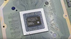
AMD will supply a semi-custom SoC to Sony for its next major console, "PlayStation 5." This chip will feature a graphics processor based on the "Navi" architecture, which succeeds "Vega." 2020 could also be the year when the 7 nm silicon fabrication process achieves some maturity and makes up most of the bulk ASIC production nodes. According to Tweaktown, Sony is closely working with AMD for the development of the "Navi" architecture itself, so versions of it are efficient enough to be deployed in console SoCs that are built to a cost. The design goal will be to enable 4K @ 60 Hz gaming, as 4K televisions will have proliferated a lot by 2020.

HWiNFO Adds Support For Upcoming AMD CPUs, GPUs, Others

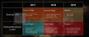
PC diagnostics tool HW Info has added support for future, as-of-yet unreleased AMD CPUs and GPUs, which seemingly confirm some earlier news on AMD's plans for their next-generation offerings. HWiNFO's v5.72 update adds support for upcoming AMD Navi GPUs, Pinnacle Ridge, 400-series motherboards (which should make their market debut alongside AMD's Zen+ CPUs), and enhanced support for AMD's Starship, Matisse and Radeon RX Vega M. We already touched upon AMD's Matisse codename in the past: it's expected to refer to the company's Zen 2 microarchitecture, which will bring architecture overhauls of the base Zen design - alongside a 7 nm process - in order to bring enhanced performance and better power consumption.

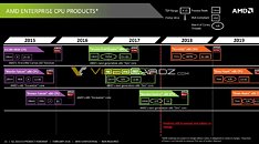
Starship, on the other hand, is a previously leaked evolution of AMD's current Naples offering that powers their EPYC server CPUs. Starship has been rumored to have been canceled, and then put back on the product schedule again; if anything, its inclusion in HWiNFO's latest version does point towards it having made the final cut, after all. Starship will bring to businesses an increased number of cores and threads (48/96) compared to Naples' current top-tier offering (32/64), alongside a 7 nm manufacturing process.

Lesson from the Crypto/DRAM Plagues: Build Future-Proof

As someone who does not mine crypto-currency, loves fast computers, and gaming on them, I find the current crypto-currency mining craze using graphics cards nothing short of a plague. It's like war broke out, and your government took away all the things you love from the market. All difficult times teach valuable lessons, and in this case, it is "Save up and build future-proof."

When NVIDIA launched its "Pascal" GPU architecture way back in Summer 2016, and AMD followed up, as a user of 2x GeForce GTX 970 SLI, I did not feel the need to upgrade anything, and planned to skip the Pascal/Polaris/Vega generation, and only upgrade when "Volta" or "Navi" offered something interesting. My pair of GTX 970 cards are backed by a Core i7-4770K processor, and 16 GB of dual-channel DDR3-1866 memory, both of which were considered high-end when I bought them, around 2014-15.

Throughout 2016, my GTX 970 pair ate AAA titles for breakfast. With NVIDIA investing on advancing SLI with the new SLI-HB, and DirectX 12 promising a mixed multi-GPU utopia, I had calculated a rather rosy future for my cards (at least to the point where NVIDIA would keep adding SLI profiles for newer games for my cards to chew through). What I didn't see coming was the inflection point between the decline of multi-GPU and crypto-plague eating away availability of high-end graphics cards at sane prices. That is where we are today.

AMD Reveals CPU, Graphics 2018-2020 Roadmap at CES

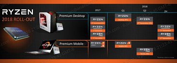
AMD at CES shed some light on its 2018 roadmap, while taking the opportunity to further shed some light on its graphics and CPU projects up to 2020. Part of their 2018 roadmap was the company's already announced, across the board price-cuts for their first generation Ryzen processors. This move aims to increase competitiveness of its CPU offerings against rival Intel - thus taking advantage of the blue giant's currently weakened position due to the exploit saga we've been covering. This move should also enable inventory clearings of first-gen Ryzen processors - soon to be supplanted by the new Zen+ 12 nm offerings, which are expected to receive a 10% boost to power efficiency from the process shrink alone, while also including some specific improvements in optimizing their performance per watt profile. These are further bound to see their market introduction in March, and are already in the process of sampling.

On the CPU side, AMD's 2018 roadmap further points towards a Threadripper and Ryzen Pro refresh in the 2H 2018, likely in the same vein as their consumer CPUs that we just talked about. On the graphics side of their 2018 roadmap, AMD focused user's attention in the introduction of premium Vega offerings in the mobile space (with HBM2 memory integration on interposer, as well), which should enable the company to compete against NVIDIA in the discrete graphics space for mobile computers. Another very interesting tidbit announced by AMD is that they would be skipping the 12 nm process for their graphics products entirely; the company announced that it will begin sampling of 7 nm Vega products to its partners, but only on the Instinct product line of machine learning accelerators. We consumers will likely have to wait a little while longer until we see some 7 nm graphics cards from AMD.

AMD Navi Found Secretly Hiding in Linux Drivers

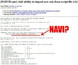
We know AMD has been doing a great job keeping the lid on their Navi architecture with information being scarce at the moment. Aside from knowing that Navi is being fabricated on the 7 nm process, it is possible that the microarchitecture will quite possibly support next-generation memory like GDDR6 or HBM3. In a Navi discussion on the Beyond3D forums, a user found an entry in a Linux driver dated back to July that apparently mentions AMD's upcoming architecture - not by its real name, of course. The code is to add support for importing new asic definitions from a text file as opposed to adding support in code. Tom St Denis, a software engineer at AMD, listed the output that would be generated by using this functionality. However, the entry that caught our attention reads: new_chip.gfx10.mmSUPER_SECRET.enable [0: 0]. If our memory serves us right, the codename for Vega was GFX9. So by logic, Navi should carry the GFX10 codename. Obviously, the SUPER_SECRET part further backs up our theory or maybe AMD's just trolling us. The red team has been hiring personnel for their GFX10 projects, so we can assume they're working diligently to release Navi some time next year.

AMD "Navi" GPU by Q3-2018: Report

AMD is reportedly accelerating launch of its first GPU architecture built on the 7 nanometer process, codenamed "Navi." Graphics cards based on the first implementation of "Navi" could launch as early as by Q3-2018 (between July and September). Besides IPC increments with its core number-crunching machinery, "Navi" will introduce a slew of memory and GPU virtualization technologies.

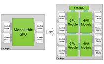
AMD will take its multi-chip module (MCM) approach of building high-performance GPUs a step further, by placing multiple GPU dies with their HBM stacks on a single package. The company could leverage its InfinityFabric as a high-bandwidth interconnect between the GPU dies (dubbed "GPU module"), with an I/O controller die interfacing the MCM with the host machine. With multi-GPU on the decline for games, it remains to be seen how those multiple GPU modules are visible to the operating system. In the run up to "Navi," AMD could give its current "Vega" architecture a refresh on a refined 14 nm+ process, to increase clock speeds.

AMD to Build 2nd Gen. Ryzen and Radeon Vega on GloFo 12nm

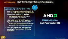
Not to be held back by silicon fabrication process limitations like in the past, AMD will build its second-generation Ryzen CPUs and Radeon Vega GPUs on the new 12 nanometer LP (low power) FinFET process by GlobalFoundries. From the looks of it, "2nd generation Ryzen" doesn't seem to be the same as "Zen2" (a micro-architectural advancement due to be built on the 7 nm process), and is more likely an optical shrink of existing 14 nm IP to the 12 nm process, giving AMD the headroom to increase yields, and clock speeds across the board. The 12 nm switch allows AMD to roll out a new "generation" of Ryzen processors as early as the first half of 2018.

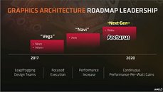
The "Vega 10" silicon could be another key piece of AMD IP on the receiving end of an optical shrink to 12 nm, which will give AMD much needed power savings, letting it increase clock speeds, and probably implement faster standards of HBM2 memory, such as 2.00 GT/s. AMD will likely label this shrunk down silicon "Vega 20." There's also the possibility of AMD building a bigger new GPUs altogether. In 2019, the company will give its CPU and GPU lineups major micro-architectural upgrades, and the switch to the 7 nm node. The new "Zen2" micro-architecture with IPC increases and new ISA instruction-sets, will be launched on the CPU side, and the new "Navi" graphics architecture will take center-stage.

Intel Says AMD EPYC Processors "Glued-together" in Official Slide Deck

So, yes, Intel, I think the AMD engineers who have developed the Zen architecture from the ground-up would take issue with that. Especially when AMD's "Glued-together" dies actually wipe the proverbial floor with the blue company's chips in power-performance ratios, and deliver much better multi-threaded performance than Intel's offerings. Not bad for a "Glued-together" solution, I'd say.

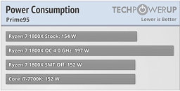
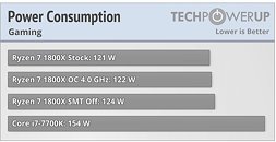
Our resident W1zzard had this to say regarding AMD's latest CPUs: "The SenseMi power-management system seems to be working well in idle, with the 8-core machine drawing the same amount of power as Intel's quad-core "Kaby Lake" machine." And "At stock speeds, the energy-efficiency of Ryzen is truly phenomenal. Prime95 loads all cores and threads on the chip, and the Ryzen ends up with as much power draw as the quad-core Intel i7-7700K. The high power draw result of the overclocked chip is due to the increased voltage needed to achieve stable operation." And let's not forget this: This is epic. We're assuming you've sifted through our game-test results before seeing this page, and so you'll find that the gaming power draw of the 8-core Ryzen makes Intel's quad-core i7-7700K look bad. Power draw is as much as 30W lesser! Ryzen is hands down the most energy-efficient performance CPU AMD ever made, and easily outclasses Intel's 14 nm "leadership." Good show."

AMD to Continue Working With TSMC, GLOBALFOUNDRIES on 7 nm Ryzen

In the Q&A section of their 2017 Financial Analyst Day, AMD CEO Lisa Su answered an enquiry from a Deutsche-bank questioner regarding the company's aggressive 7 nm plan for their roadmap, on which AMD seems to be balancing its process shrinkage outlook for the foreseeable future. AMD will be developing their next Zen architecture revisions on 7 nm, alongside a push for 7 nm on their next-generation (or is that next-next generation?) Navi architecture. This means al of AMD's products, consumer, enterprise, and graphics, will be eventually built on this node. This is particularly interesting considering AMD's position with GLOBALFOUNDRIES, with which AMD has already had many amendments to their Wafer Supply Agreement, a remain of AMD's silicon production division spin-off, the latest of which runs from 2016 to 2020.

As it is, AMD has to pay GLOBALFOUNDRIES for its wafer orders that go to other silicon producers (in this case, TSMC), in a quarterly basis since the beginning of 2017, based on the volume of certain wafers purchased from another wafer foundry. In addition, AMD has annual wafer purchase targets from 2016 through the end of 2020, fixed wafer prices for 2016, and a framework for yearly wafer pricing in this amendment, so the company is still bleeding money to GLOBALFOUNDRIES. However, AMD is making the correct decision in this instance, I'd wager, considering GLOBALFOUNDRIES' known difficulties in delivering their process nodes absent of quirks.

AMD to Detail Vega, Navi, Zen+ on May 16th - Laying Out a Vision

Reports are circling around the web regarding an AMD meeting featuring some of its higher ups - namely, CEO Lisa Su, head of Radeon Technologies Group Raja Koduri, and AMD's CTO Mark Papermaster happening on the 16th of May. The purpose of this meeting seems to be to discuss AMD's inflexion point, and lay out a vision for the company's future, supported on its upcoming products: the too-long-awaited Vega, its successor Navi, and the natural evolution of the company's current Zen processors, tentatively identified as Zen+.

Naturally, a company such as AMD has its roadmap planned well in advance, with work on next-generation products and technologies sometimes even running in parallel with current-generation product development. It's just a result of the kind of care, consideration, time and money that goes into making new architectures that makes this so. And while some would say Vega is now approaching a state akin to grapes that have been hanging for far too long, AMD's next graphics architecture, Navi, and its iterations on Zen cores, which the company expect to see refreshes in a 3-to-5-year period, are other matters entirely. Maybe we'll have some more details regarding the specific time of Vega's launch (for now expected on Computex), as well as on when AMD is looking to release a Zen+ refresh. I wouldn't expect much with regards to Navi - perhaps just an outline on how work is currently underway with some comments on the expectations surrounding Global Foundries' 7 nm process, on which Navi is expected to be built. And no, folks, this isn't a Vega launch. Not yet.

AMD Vega 10, Vega 20, and Vega 11 GPUs Detailed

AMD CTO, speaking at an investors event organized by Deutsche Bank, recently announced that the company's next-generation "Vega" GPUs, its first high-end parts in close to two years, will be launched in the first half of 2017. AMD is said to have made significant performance/Watt refinements with Vega, over its current "Polaris" architecture. VideoCardz posted probable specs of three parts based on the architecture.

AMD will begin the "Vega" architecture lineup with the Vega 10, an upper-performance segment part designed to disrupt NVIDIA's high-end lineup, with a performance positioning somewhere between the GP104 and GP102. This chip is expected to be endowed with 4,096 stream processors, with up to 24 TFLOP/s 16-bit (half-precision) floating point performance. It will feature 8-16 GB of HBM2 memory with up to 512 GB/s memory bandwidth. AMD is looking at typical board power (TBP) ratings around 225W.

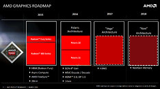
AMD's GPU Roadmap for 2016-18 Detailed

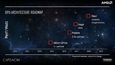
AMD finalized the GPU architecture roadmap running between 2016 and 2018. The company first detailed this at its Capsaicin Event in mid-March 2016. It sees the company's upcoming "Polaris" architecture, while making major architectural leaps over the current-generation, such as a 2.5-times performance/Watt uplift and driving the company's first 14 nanometer GPUs; being limited in its high-end graphics space presence. Polaris is rumored to drive graphics for Sony's upcoming 4K Ultra HD PlayStation, and as discrete GPUs, it will feature in only two chips - Polaris 10 "Ellesmere" and Polaris 11 "Baffin."

"Polaris" introduces several new features, such as HVEC (h.265) decode and encode hardware-acceleration, new display output standards such as DisplayPort 1.3 and HDMI 2.0; however, since neither Polaris 10 nor Polaris 11 are really "big" enthusiast chips that succeed the current "Fiji" silicon, will likely make do with current GDDR5/GDDR5X memory standards. That's not to say that Polaris 10 won't disrupt current performance-thru-enthusiast lineups, or even have the chops to take on NVIDIA's GP104. First-generation HBM limits the total memory amount to 4 GB over a 4096-bit path. Enthusiasts will have to wait until early-2017 for the introduction of the big-chip that succeeds "Fiji," which will not only leverage HBM2 to serve up vast amounts of super-fast memory; but also feature a slight architectural uplift. 2018 will see the introduction of its successor, codenamed "Navi," which features an even faster memory interface.

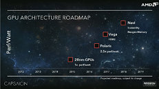
AMD Unveils GPU Architecture Roadmap, "Polaris" to Skip HBM2 Memory?

Alongside its big Radeon Pro Duo flagship graphics card launch, AMD unveiled its GPU architecture roadmap that looks as far into the future as early-2018. By then, AMD will have launched as many as three new GPU architectures. It begins with the launch of its 4th generation Graphics CoreNext architecture, codenamed "Polaris," in mid-2016. Built on the 14 nm FinFET process, "Polaris" is expected to offer a whopping 2.5x increase in performance-per-Watt for AMD, compared to its current GCN 1.2 architecture on 28 nm.

Hot on Polaris' heels, in early-2017, AMD plans to launch the "Vega" GPU architecture. While this appears to offer a 50% increase in performance-per-Watt over Polaris, its highlight is HBM2 memory. Does this mean that AMD plans to skip HBM2 on Polaris, and stick to GDDR5X? Could AMD be opting for a similar approach to NVIDIA, by launching its performance-segment GPU first as an enthusiast product, giving it a free run on the markets till early-2017, and then launching a Vega-based big-chip with HBM2 memory, taking over as the enthusiast-segment product? Some time in early-2018, AMD will launch the "Navi" architecture, which appears to offer a 2.5x performance-per-Watt lead over Polaris, taking advantage of an even newer memory standard.
Return to Keyword Browsing
Dec 18th, 2024 00:43 EST change timezone

New Forum Posts

Popular Reviews

Controversial News Posts